Why Don't We Have L5 CPU Caches?
A deep dive into CPU cache hierarchy: why we can't just build one big cache, and why physics prevents L5 from existing.
Introduction
Have you ever wondered about a seemingly trivial question: why do processors have cache levels? Why not just use one large cache? The answer intertwines semiconductor physics, processor architecture history, and how compilers learned to utilize memory hierarchy.
Physics Dictates Architecture
The processor isn't an abstract computing device but rather a real piece of silicon, roughly the size of a thumbnail, containing billions of transistors. When data travels from memory to registers, electrical signals propagate through metallic conductors measuring millimeters or centimeters. At clock frequencies of 3-4 GHz, this distance matters — signals travel only about 10 centimeters per cycle, and less within chip circuitry due to resistance and parasitic capacitance.
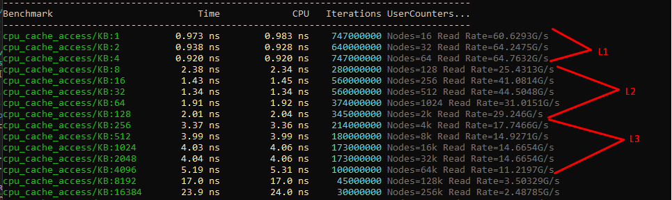
Signal propagation through conductors involves physical delays, resistance, and power consumption proportional to distance. This physical constraint makes a single enormous cache impractical. Access time increases with distance from the core, making hierarchical organization essential.
If you took all modern CPU cache — roughly 2MB of L1 + L2 combined — and created one large storage unit, the core would need to wait for signals to reach possibly the farthest corner and return. Complexity in addressing schemes increases, energy consumption per access grows, and density suffers. Fast SRAM cells in L1 consume vastly more area than slower L2 cache cells, forcing designers toward natural hierarchy: small fast cache near the core, progressively larger and slower levels further away.
The Christmas Tree Analogy
Imagine decorating a Christmas tree with ornaments from multiple storage locations:
- L1 Cache: A small box in your hands containing five or six recently selected ornaments — accessible in seconds.
- L2 Cache: A cardboard box on a nearby chair requiring reaching and searching — noticeably slower but still accessible.
- L3 Cache: A large bag in another room requiring getting up and searching through reserves — time-consuming but containing most items.
- RAM (DRAM): An old dresser in the attic — accessing it means finding a ladder, climbing up, searching through accumulation — work completely stops while you search.
You wouldn't replace all four storage locations with one giant shelf in the room. The small box in hand loses its advantage when it becomes one corner of an enormous shelf requiring reaching anyway.
Historical Context
Cache hierarchy didn't emerge immediately. Late-1970s processors lacked hardware cache entirely, accessing external memory directly with negligible latency difference.
Early 1980s brought changes as processors accelerated faster than memory. Manufacturers added small caches to circuit boards, then directly onto chips.
1989: Intel i486 became the first mass-market processor with embedded L1 cache on the die, unified for instructions and data. Simultaneously, compilers like Borland C++ began applying data locality concepts, optimizing variable placement and structure field ordering empirically without formal cache models.
1993: Pentium split cache into separate instruction (L1I) and data (L1D) versions, reflecting their fundamentally different physical requirements. Compilers refined code/data section separation, with GCC adding function alignment optimizations.
1995: Pentium Pro moved L2 cache to separate chips, making hierarchy explicit and two-level.
2008: Nehalem established the familiar three-level scheme: separate L1I and L1D caches, unified L2 per core, and shared L3.
LLVM, appearing during this period, incorporated these lessons — initially designed considering this hierarchy with passes for loop tiling, prefetching, and hot data layout.
Different Access Patterns Require Different Structures
L1D (data cache) and L1I (instruction cache) are fundamentally different devices with conflicting requirements, preventing simple merging despite identical sizes.
L1D reads and writes individual elements (1-8 bytes), requiring multiple simultaneous read/write ports, store forwarding, and coherence tracking across cores.
L1I remains read-only from the core's perspective, allowing simplified design but demanding enormous throughput — Intel Core i7 can fetch 16 bytes per cycle from L1I, yielding approximately 50 GB/s bandwidth just for instructions.
Combining peak instruction and data traffic would create mutually exclusive requirements, forcing compromise on both.
Private vs. Shared Cache
Private versus shared space matters fundamentally. L1D is private, enabling cores to read/write without coordination — this privacy provides single-cycle access critical for pipelines. L1I is similarly private.
L2 remains private but handles some inter-core traffic, affecting speed. L3 is physically shared, requiring coordination through coherence protocols.
Cache Coherence Protocols
The article details various coherence protocols that manage cache state across multiple cores:
- MSI (Modified, Shared, Invalid) — the basic three-state protocol
- MESI (Modified, Exclusive, Shared, Invalid) — adds Exclusive state to reduce bus traffic
- MOESI (Modified, Owner, Exclusive, Shared, Invalid) — adds Owner state for dirty sharing
- MESIF (Modified, Exclusive, Shared, Invalid, Forward) — Intel's variant for QPI interconnect
- MOSI, MOESIF — further extensions
- Stanford DASH, SGI ODP — directory-based protocols for larger systems
Each protocol adds complexity while managing how multiple cores see consistent memory state. Earlier cache levels reduce access frequency sufficiently that coordination becomes non-bottlenecking.
How Cache Hierarchy Impacts Programming
This matters practically because sequential, predictable code runs orders of magnitude faster than chaotic equivalents.
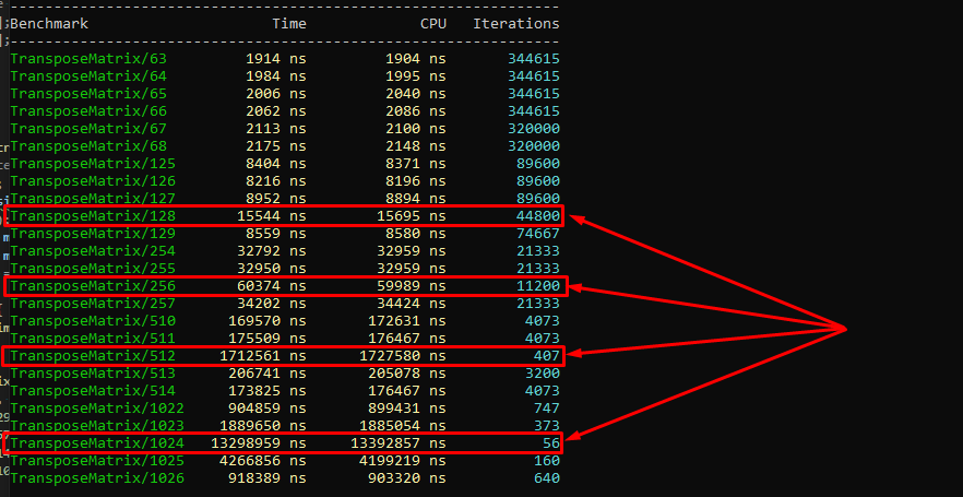
Traversing 2D arrays row-by-row versus column-by-column shows dramatic differences: proper ordering loads data in single cache lines spanning multiple iterations; reversed iteration causes cache misses, requiring L3/DRAM trips. Performance differences on real tasks like matrix multiplication or sorting can exceed ten-fold, which is why compilers now perform loop interchange, loop tiling, and prefetch insertion automatically.
The Array-of-Structures (AoS) versus Structure-of-Arrays (SoA) distinction flows directly from L1 cache operating in 64-byte lines. Processing single object fields while objects consume 128 bytes loads unnecessary data, halving effective cache capacity.
Do We Need L4 Cache?
If hierarchy logic — each level providing benefits through volume at acceptable latency — holds, why stop at three?
L4 makes sense only when working sets systematically exceed L3 capacity while remaining "hot" enough that DRAM access becomes bottlenecking. This describes specific scenarios: server databases, large telemetry tasks, heavy rendering applications — not typical desktop workloads where 8-32MB L3 exceeds most working sets.
Nevertheless, attempts exist:
Intel Haswell-GT3e (2013-2014)
Intel placed a separate 128MB eDRAM crystal beside the processor die, serving as fourth-level cache for CPU and integrated GPU simultaneously. eDRAM latency exceeded SRAM caches but proved several times faster than DDR3/DDR4, yielding 2-3x improvements for film editing and heavy rendering — transforming 12-14 hour film processing into several hours.
Compilers remained unaware — fully transparent to software; hardware prefetchers decided placement. Intel experimented through Iris Pro to Kaby Lake before abandoning it: manufacturing complexity and costs made it too niche.
AMD 3D V-Cache
AMD's approach stacks additional SRAM crystals directly on top of the compute chip. While AMD positions it as expanded L3, it physically represents separate crystals — architecturally functioning as L4. The technology proved transformative for gaming workloads where slightly larger cache dramatically reduces memory latency for game physics and AI calculations.
HBM (High Bandwidth Memory)
For server processors, HBM provides very wide-bus memory integrated alongside the processor die. Functionally L4 regarding latency positioning, certain server tasks achieved 50% performance improvements, making it standard in server segments like AMD's EPYC with 3D V-Cache and Intel's server platforms.

Compiler support for explicit L4 never materialized; all operate on "hot data fits in cache" models without specifying levels. Automatic optimizations like loop tiling parametrize by cache-line size and approximate level sizes through flags like -mtune=skylake, not explicit hierarchical models. Finer control — planning hot data placement in huge pages, explicit prefetch hints through __builtin_prefetch or _mm_prefetch — remains manual optimization territory for performance-critical cases.
L4 cache is already reality in niche scenarios but shouldn't be expected in desktop processors. Each hierarchy level adds coherence complexity, manufacturing costs, and specialized control schemes justified only when workloads require them.
L5 — Why It Doesn't Exist
L5 never appears in CPU cache hierarchies as production solutions, though five-level concepts aren't impossible — they simply hit multiple walls simultaneously.
Each new level requires simultaneous solutions: sufficiently faster than DRAM to justify existence, sufficiently cheaper than previous levels in silicon area or manufacturing costs to make sense. L4 still manages this: eDRAM and HBM provide 3-5x lower latency than DDR5 at reasonable costs. But between L4 and a hypothetical L5, there simply isn't sufficient speed or density difference to insert something fundamentally new.
Coherence Complexity
Cache coherence complexity scales nonlinearly with each shared level. Each level requires MESI/MOESI protocol complexity, introduces new race condition classes, increases reconciliation time, and creates new invalidation conflicts. Three levels represent complex but manageable engineering. Four becomes viable only for niche solutions. Five approaches the point where management complexity potentially consumes all performance gains from the additional caching.
Economic Factors
Each new level adds production costs and specialized control logic, only justified for specific workload profiles. The engineering investment required to design, validate, and manufacture a fifth cache level would be enormous — and the target market vanishingly small.
Alternative Approaches
However, the industry pursued alternative paths executing similar functions with different names:
- AMD 3D V-Cache: Formally positioned as expanded L3, physically represents separate SRAM crystals stacked above compute chips — architecturally functioning as L4
- Intel "High Bandwidth Cache" and "Memory-side Cache": Deliberately avoiding traditional numbering. In server systems, these functionally execute L5-like roles regarding latency — faster than disk but orders slower than local DRAM — though they're not hardware caches semantically but rather different address space regions with different latencies
Speculative Futures
Realistic L5 scenarios require highly heterogeneous memory systems. Future chips with multiple 3D memory levels could build chains like "SRAM → eDRAM → HBM → L5? → DDR → NVM." Academic literature describes such schemes.
IBM historically employed non-standard hierarchies in z-series mainframes with more levels than x86 convention. But for mass markets, these remain research territories rather than production solutions.
Nobody has yet devised something that sits between existing cache and DRAM that is simultaneously faster than DRAM, cheaper than existing cache, and sufficiently large to warrant its own level in the hierarchy. Until that changes, L5 remains a theoretical curiosity.