Reverse Engineering the GID Display on an Opel Astra H
A detailed reverse engineering project that intercepts signals from an Opel Astra H's GID display, decodes its protocol using a logic analyzer, and outputs the display content as composite video via an FPGA.
Introduction
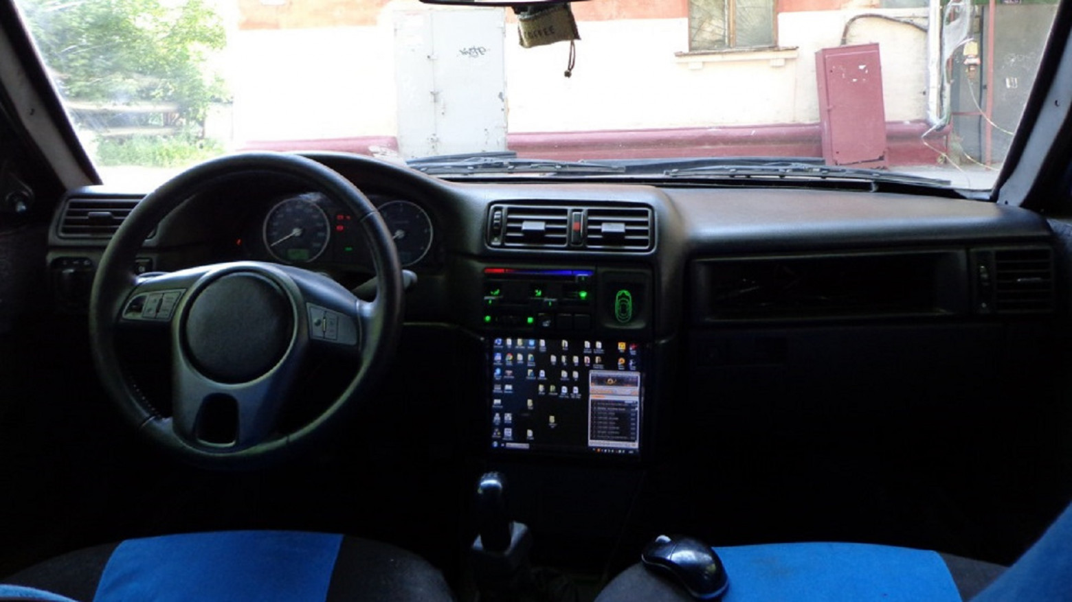
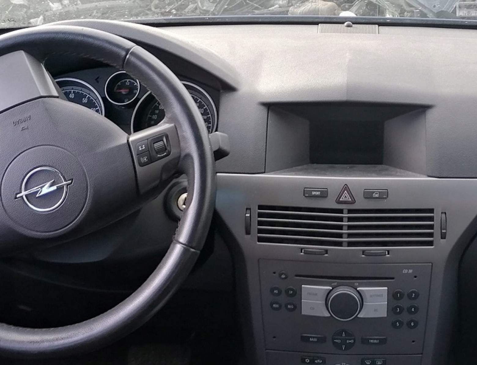
Building a car PC (CarPC) has been my passion project for over a decade. It started years ago when I built a CarPC for a Moskvich 214145 using parts from an Opel Vectra A. Now, with more experience under my belt, I returned to this hobby — this time with an Opel Astra H. The core challenge: the factory monochrome graphical display (GID) sits in a prime dashboard location, but it serves as a gateway between different CAN bus systems, making simple replacement impossible without losing climate control functionality.
The Problem
The GID display has an excellent dashboard location, but removing it creates several issues:
- The climate system stops working without the GID connected
- Having two displays in one car seems excessive and inelegant
- The display shows valuable vehicle information that you don't want to lose
I purchased an LCD matrix and an RTD2662 controller board back in 2020, but the project sat on the shelf until recently when I decided to tackle it properly.
The Approach: Intercepting Display Signals
Rather than tapping into the CAN bus data (which the "Astra H CAN hackers" community has already thoroughly decoded), I chose a different approach: intercepting the signals going directly to the display matrix itself. This way, I could capture exactly what the display shows and output it to any external screen.
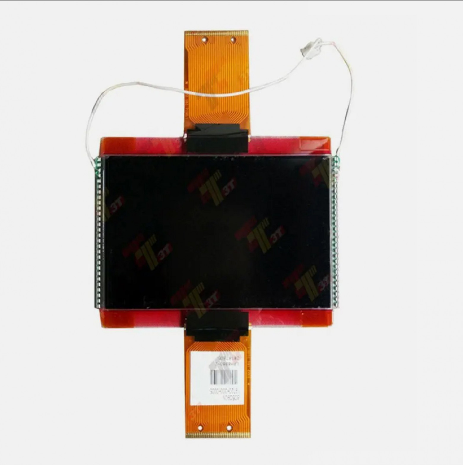
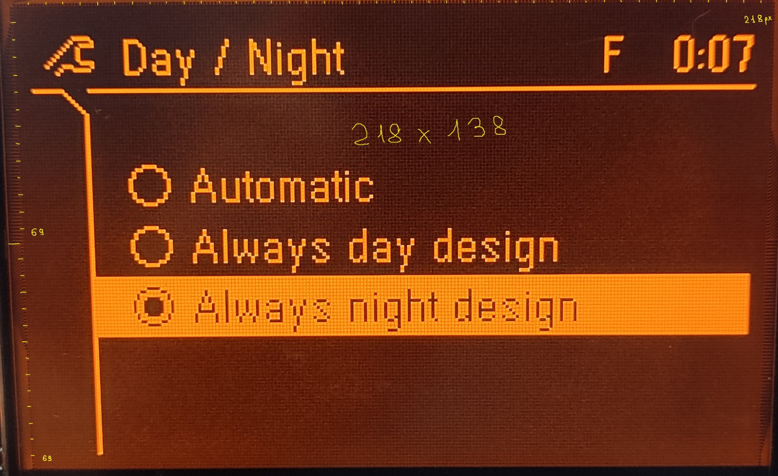
Display Specifications
The display uses an 80509CN matrix with two connectors:
- Resolution: 218 x 138 pixels
- Monochrome graphical display
- Two identical internal controllers (confirmed by testing with the display rotated 180 degrees — both halves displayed correctly)
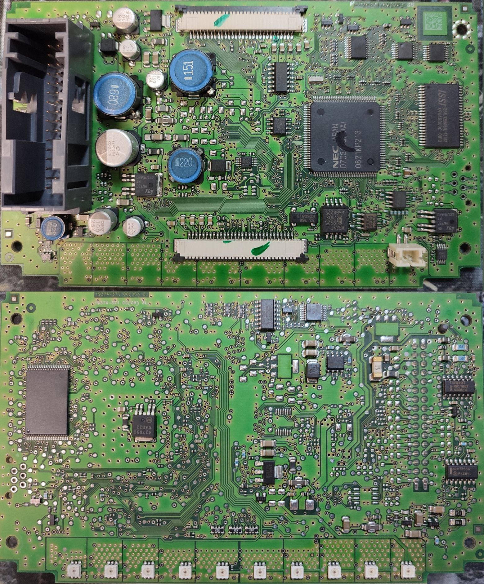
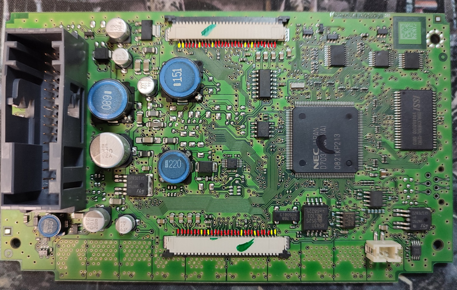
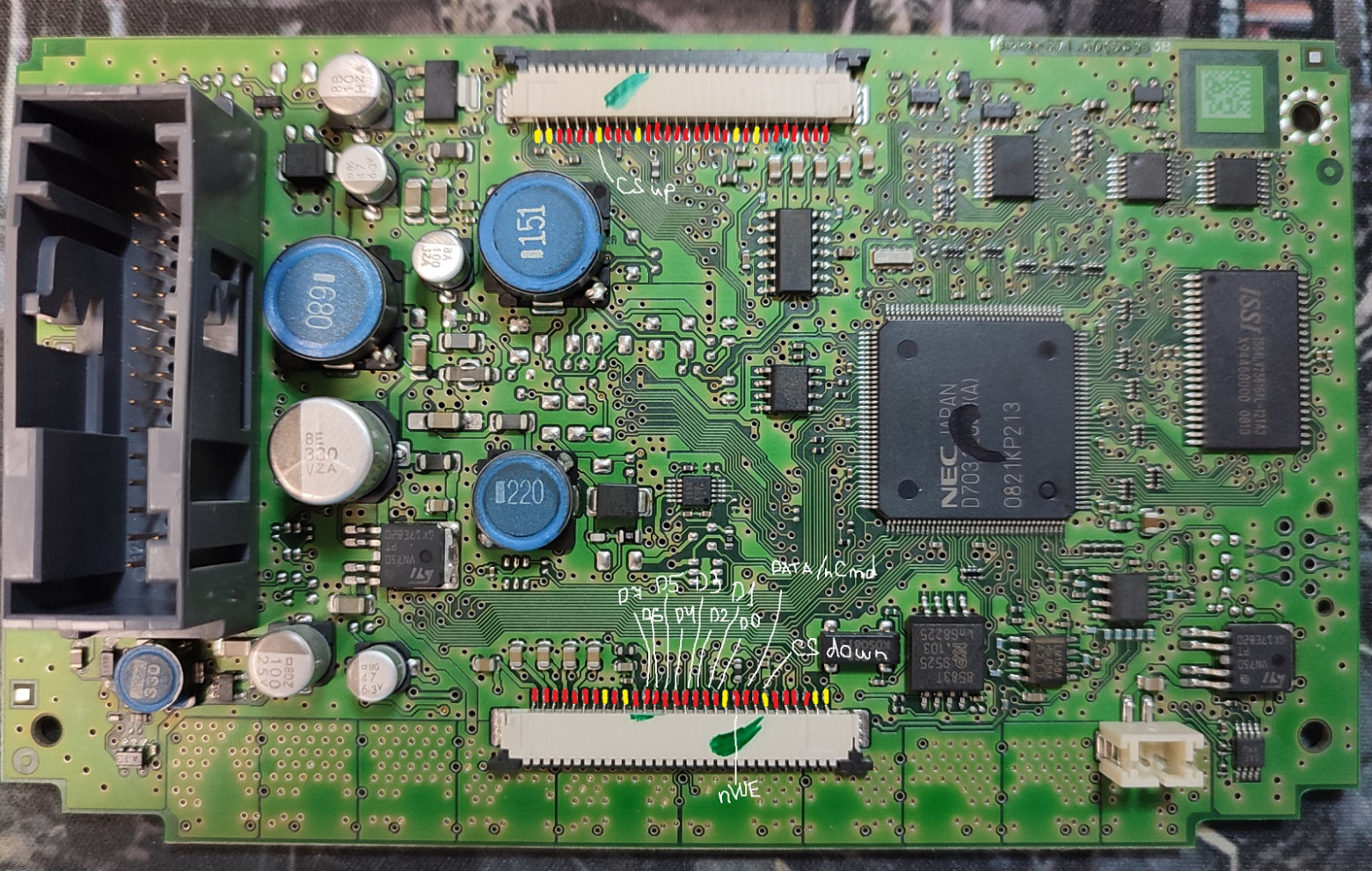
Hardware Analysis: Discovering the Pinout
Using a multimeter, I traced connections between the two connectors, color-coding my findings:
- Red — parallel connections (same signal going to both connectors)
- Yellow — unique pins for each connector
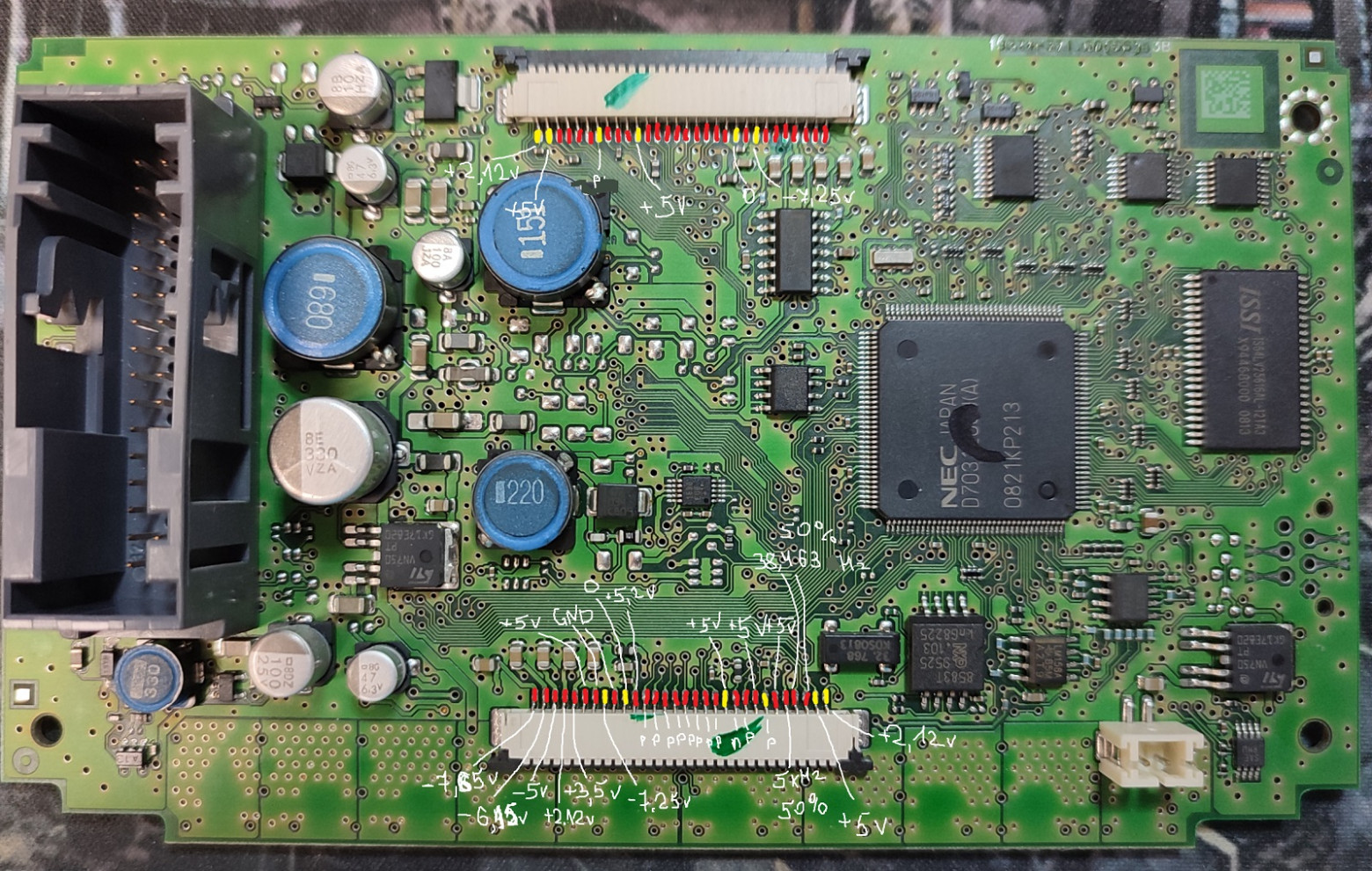
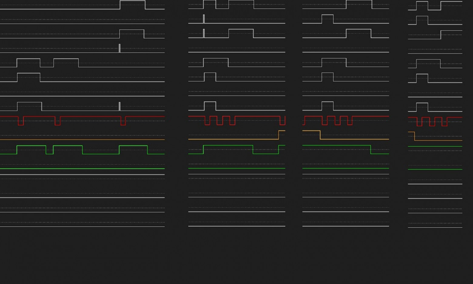
Signal Analysis with an Oscilloscope
Connecting an oscilloscope to the data lines revealed:
- An 8-bit data bus
- Separate upper/lower controller selection signals
- Stable voltage levels at 5V logic
- Clean digital signals with well-defined edges
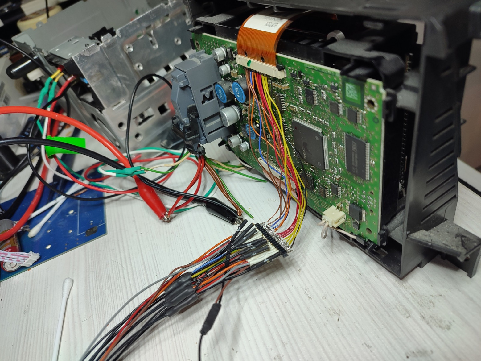
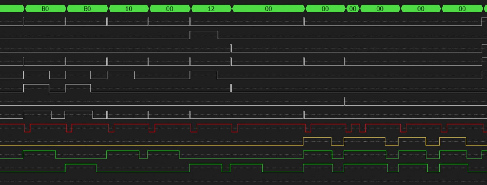
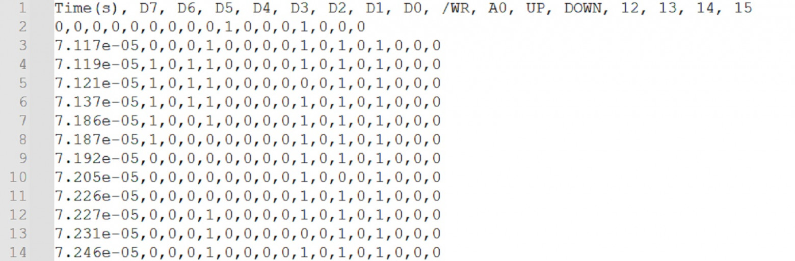
Logic Analyzer Deep Dive
Using a DSLogic analyzer with 10ns sampling rate, I captured the complete communication protocol.
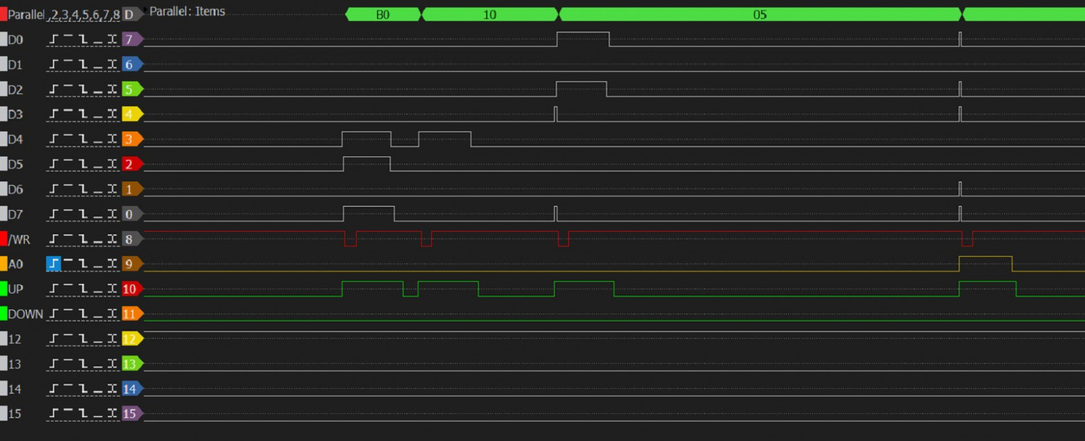
The protocol revealed eight commands for the upper display half:
[0xB0, 0x10, 0x05] [0xB1, 0x10, 0x05] [0xB2, 0x10, 0x05] [0xB3, 0x10, 0x05]
[0xB4, 0x10, 0x05] [0xB5, 0x10, 0x05] [0xB6, 0x10, 0x05] [0xB7, 0x10, 0x05]
And eight commands for the lower display half:
[0xB0, 0x12, 0x05] [0xB1, 0x12, 0x05] [0xB2, 0x12, 0x05] [0xB3, 0x12, 0x05]
[0xB4, 0x12, 0x05] [0xB5, 0x12, 0x05] [0xB6, 0x12, 0x05] [0xB7, 0x12, 0x05]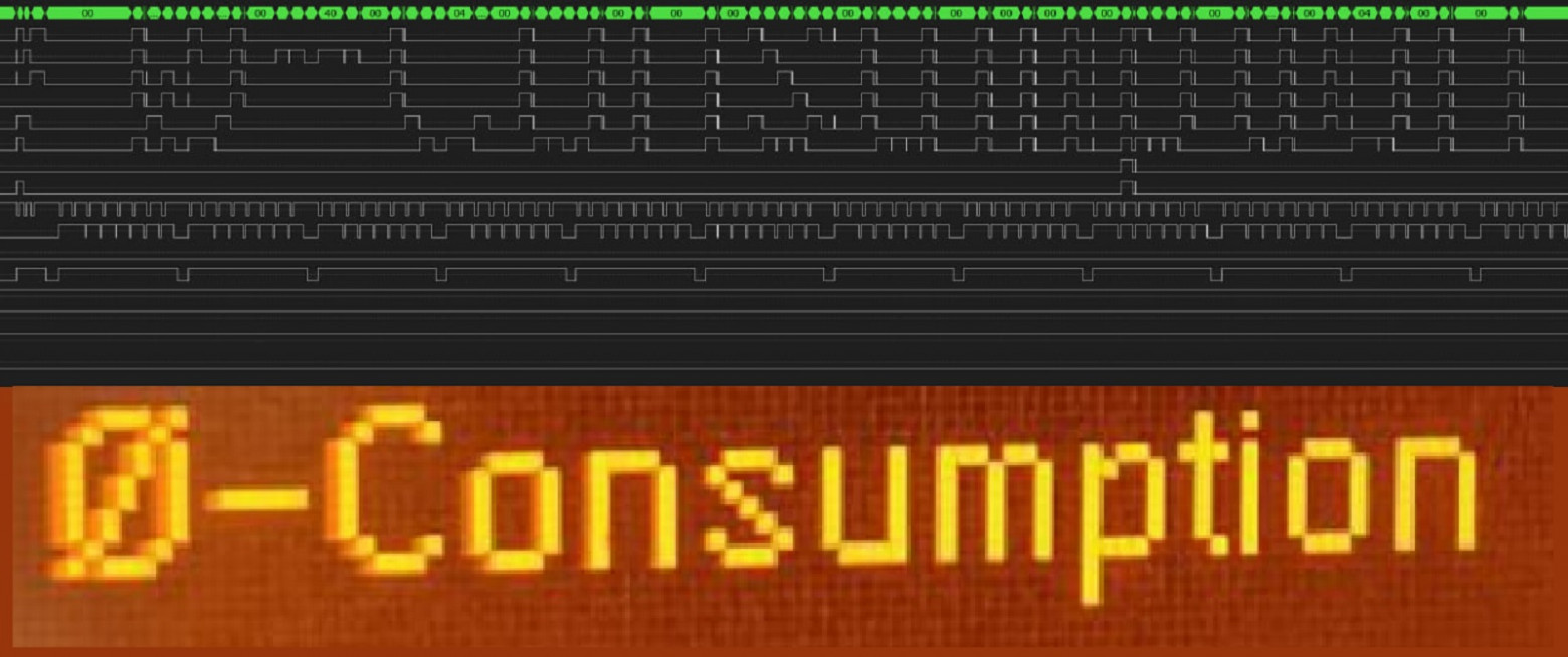
Data Structure
Each transmission consists of:
- 3 command bytes followed by 208 data bytes
- Display width: 218 pixels (with 5-pixel margins on each side)
- Refresh rate: approximately 1 Hz
- Controller identified as similar to ST7565 (but with larger resolution)
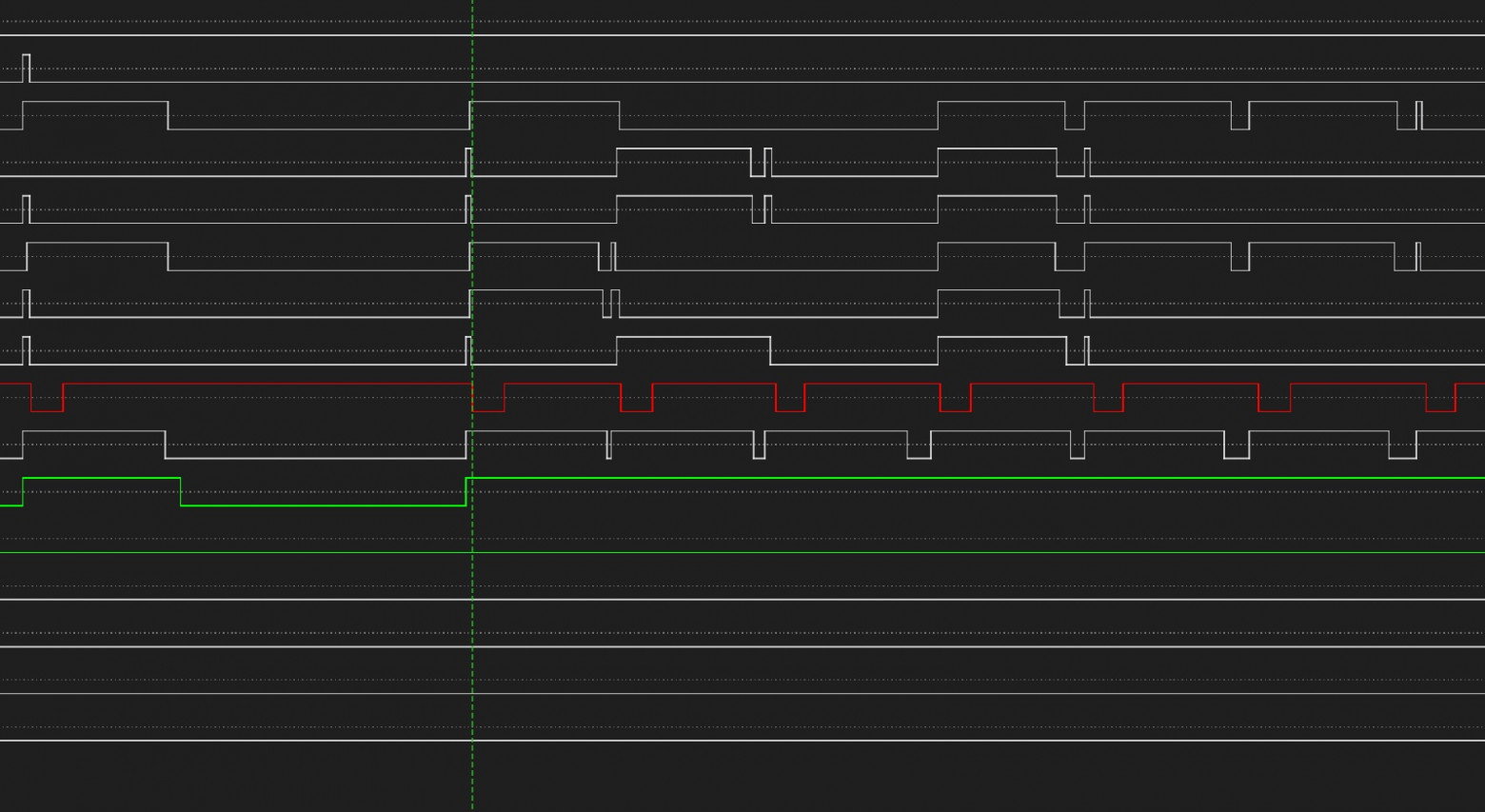
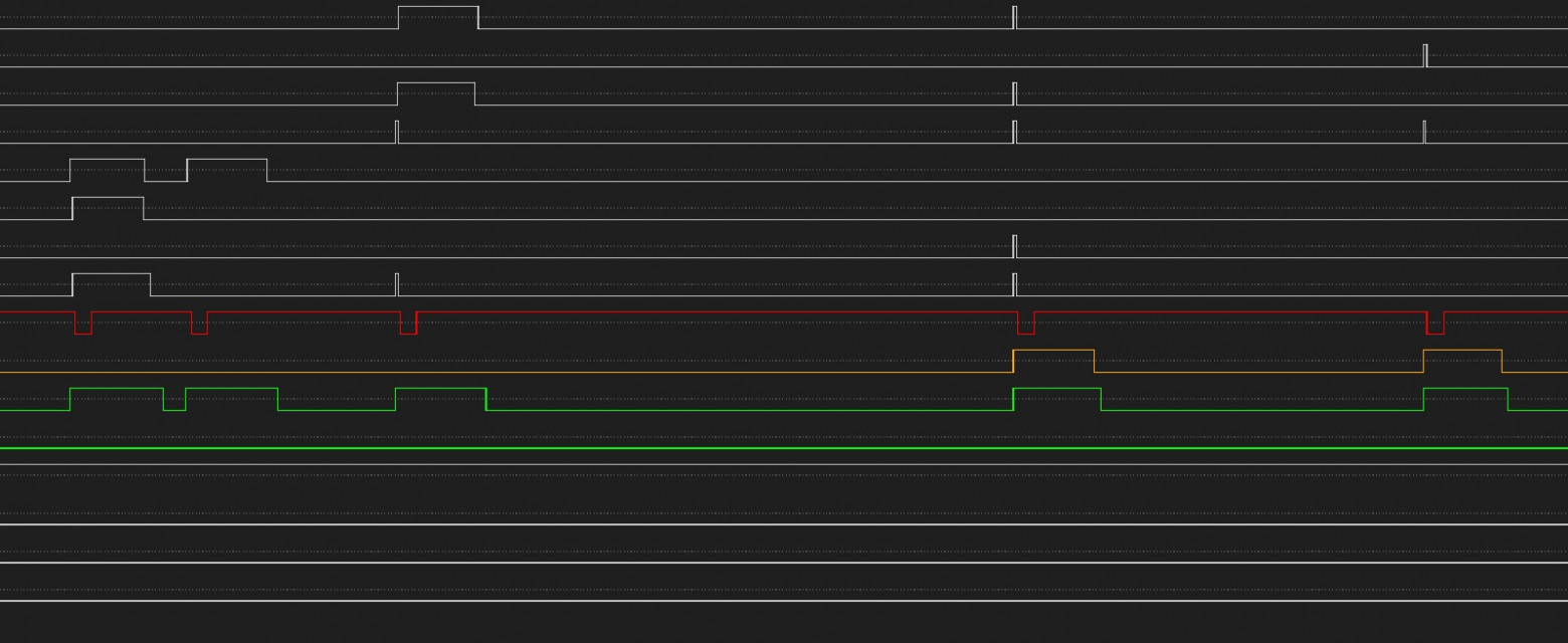
Key signal lines:
- nWE signal (negative polarity) — write enable, data latches on falling edge
- DC signal — data/command selector (distinguishes between command and pixel data)
- CS signals — chip select for upper/lower controller
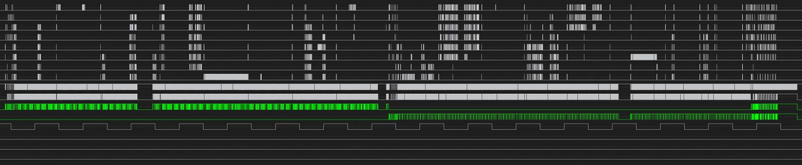
The first command byte, masked with 0xB0-0xB7, indicates the row sector. The third byte (0x05) indicates the starting column address. After 16 main transmissions (8 upper + 8 lower), padding fills the remaining pixels including off-screen areas.
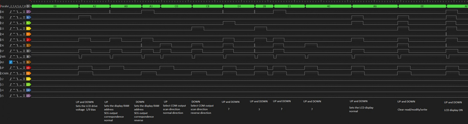
Software Decoder in C#
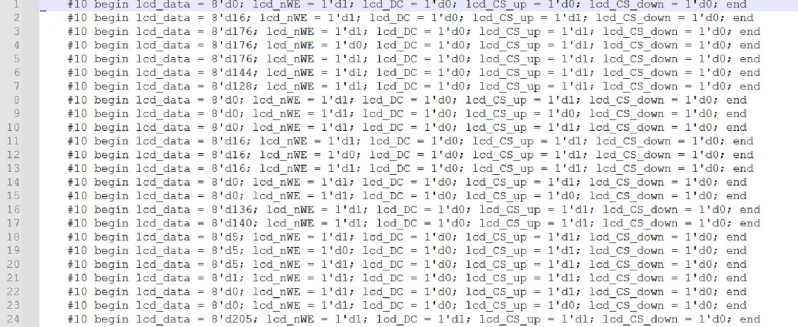
I wrote the first decoder in C# to verify my understanding of the protocol before moving to hardware.
The algorithm works as follows:
- PictureBox sized at 872 x 512 pixels (4x magnification for visibility)
- Framebuffer: 218 x 16 bytes
- Main loop scans CSV lines exported from the logic analyzer, detecting nWE falling edges
- Global variables track row and column counters plus a data validity flag
- Filter first command by mask 0xF8: if result is 0xB0, extract row number using mask 0x07
- For upper display: use row number as-is; for lower display: add 8
- Extract column address bits from the second and third command bytes
- Set validity flag for subsequent data writes; increment column counter for each write
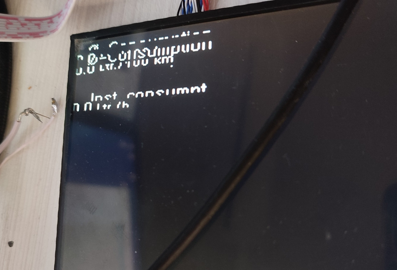
Result: the display content was successfully decoded into a bitmap format, confirming the protocol analysis was correct.
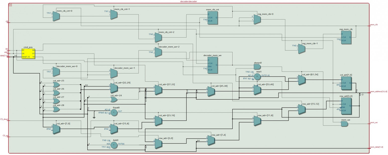
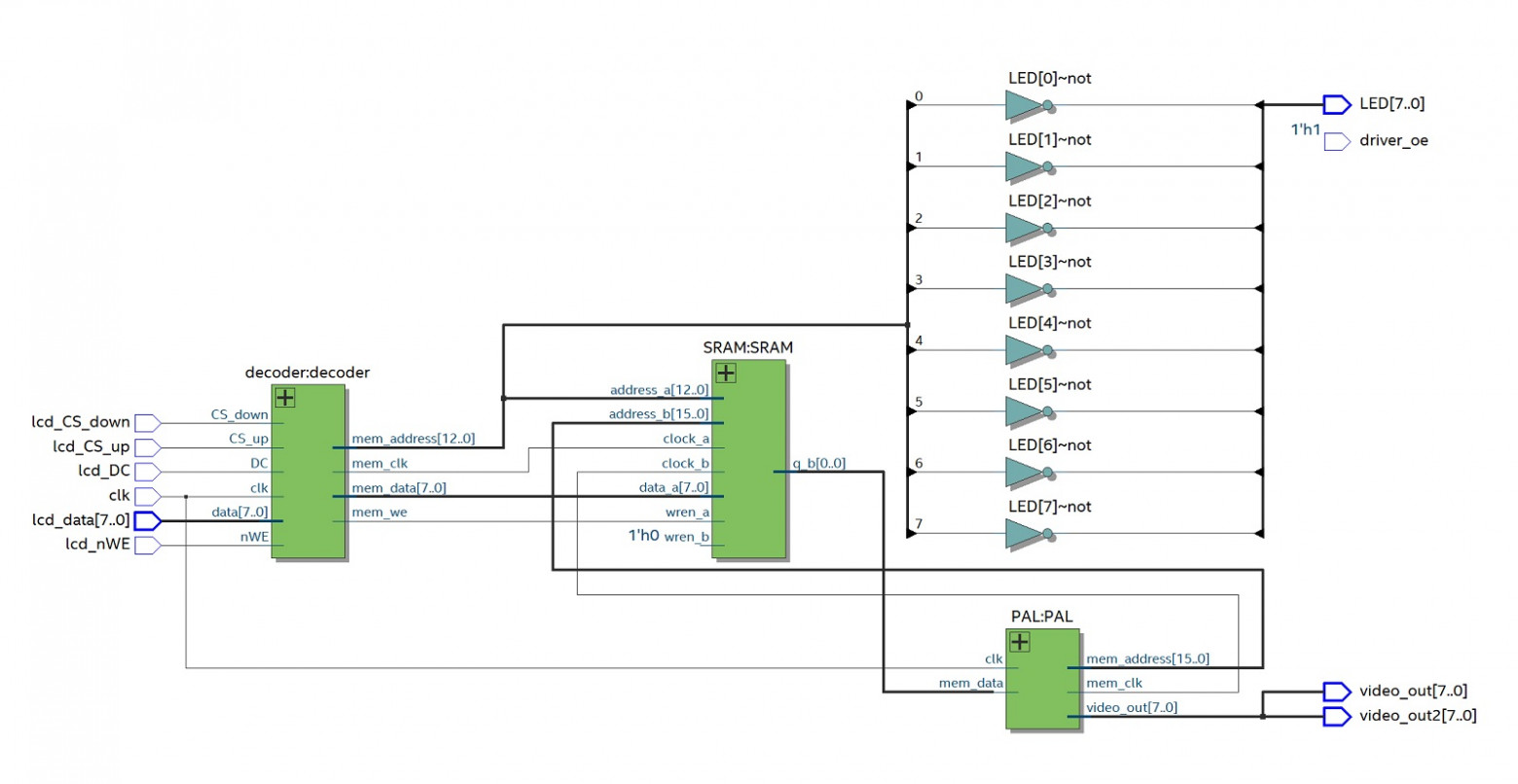
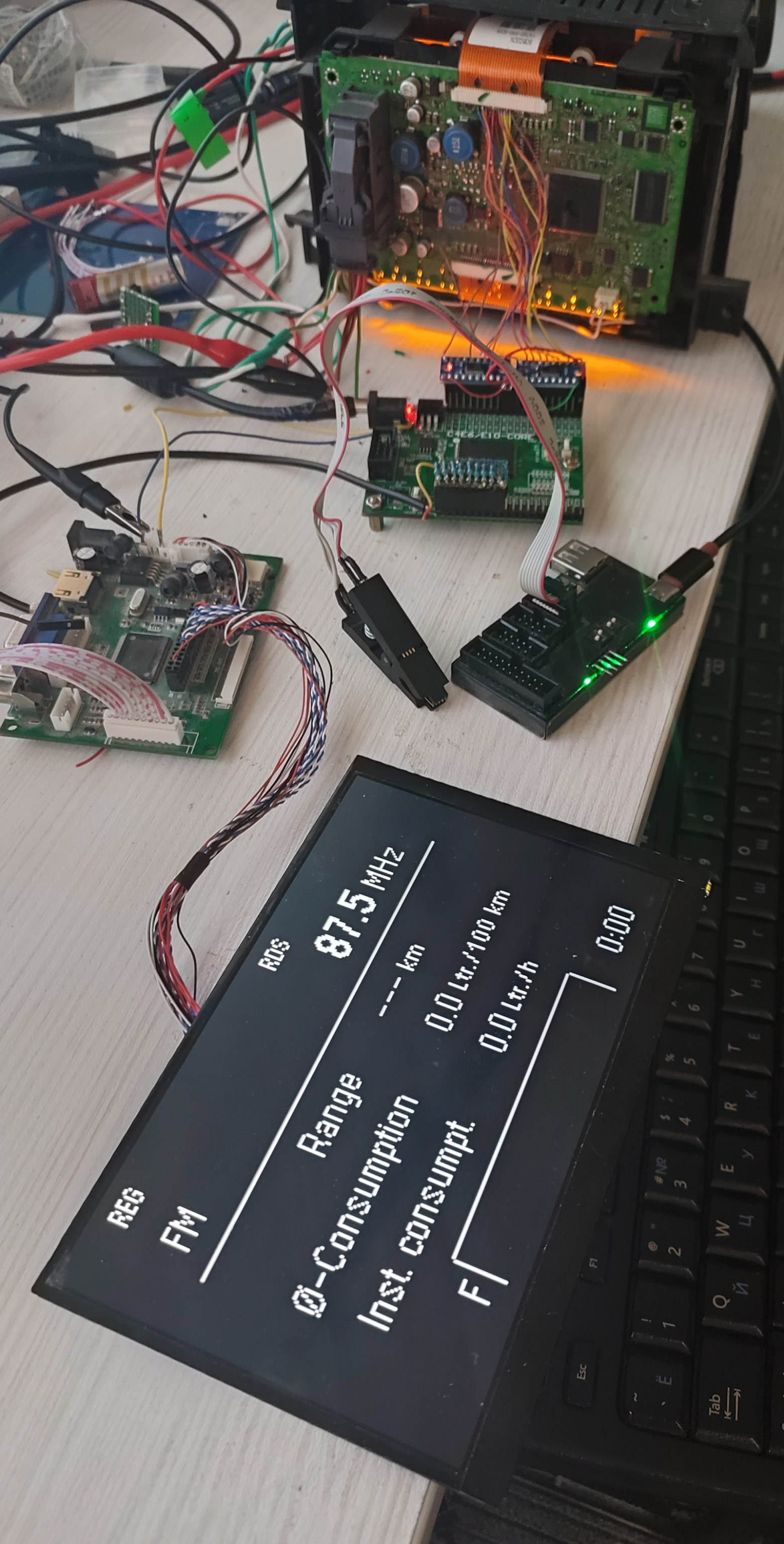
FPGA Hardware Decoder
With the protocol understood, I moved to a hardware implementation using an Altera Cyclone IV EP4CE10 FPGA.
Key implementation details:
- Built-in dual-port SRAM blocks for framebuffer storage
- 5V to 3.3V level conversion using bidirectional buffers
- OE (Output Enable) signal tied to constant logic 1
The decoder module, written in Verilog, ports the C# logic using three command-position states:
- State 0: Check for 0xB0 command pattern, extract row address
- State 1: Extract upper column address bits
- State 2: Extract lower column address bits, enable data writes
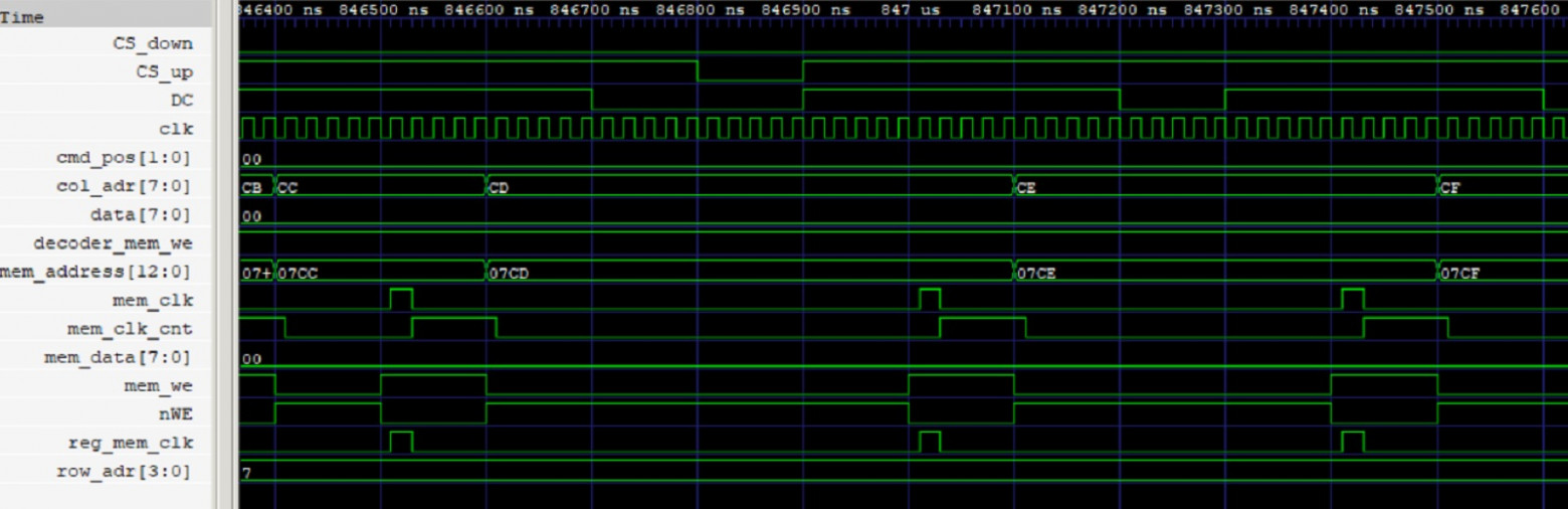
The memory interface generates address, data, write-enable, and clock signals for the SRAM. Simulation was performed using iverilog with a testbench fed by converted CSV data from the logic analyzer.
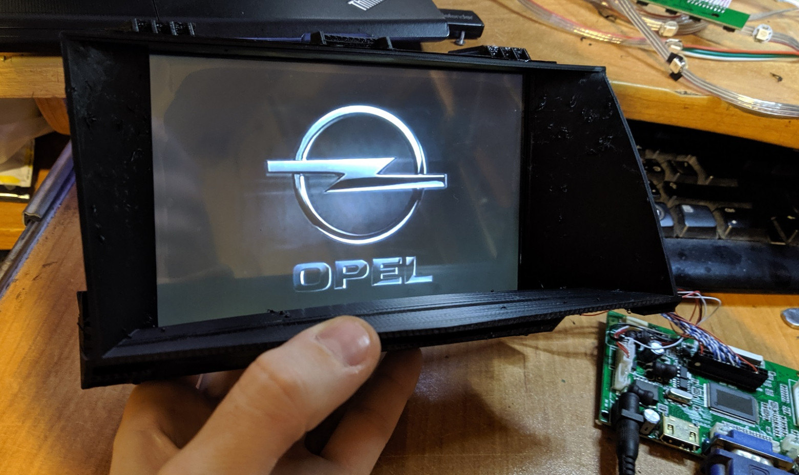
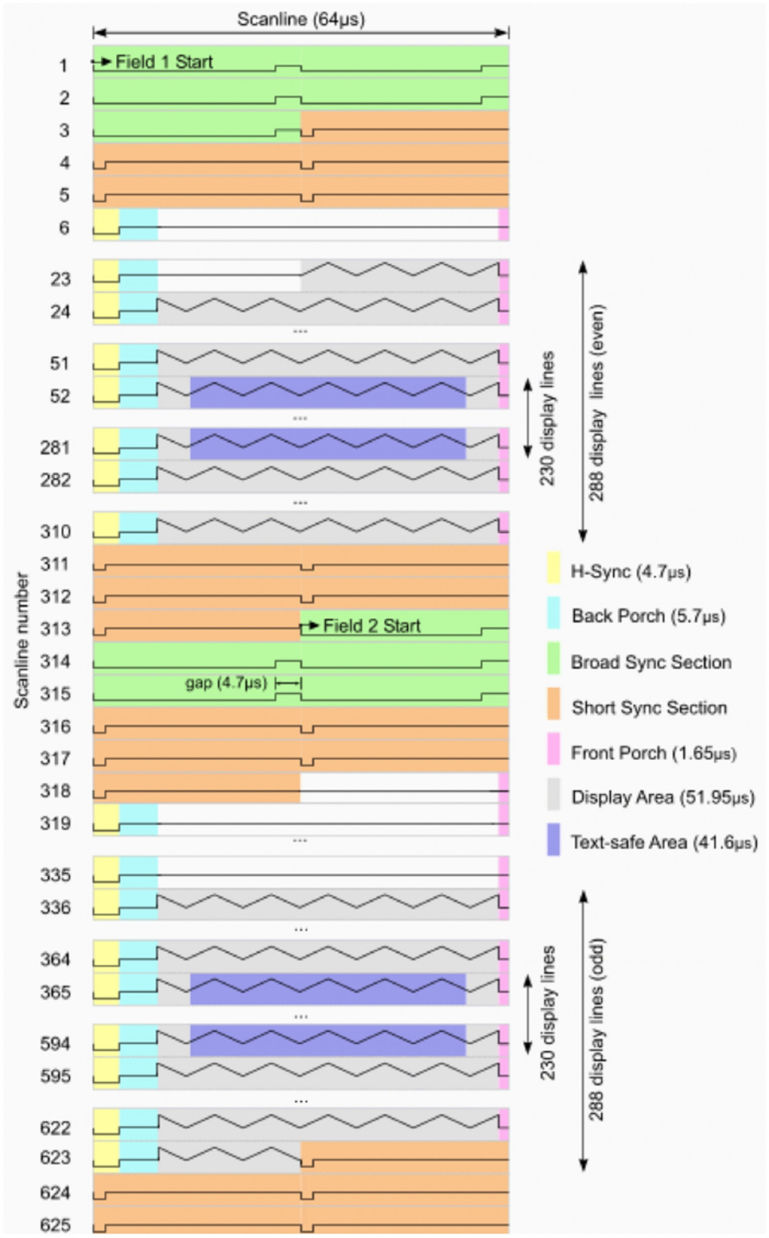
PAL/Composite Video Output
For maximum compatibility with aftermarket car head units, I chose CVBS (Composite Video Blank and Sync) output — virtually every car display supports this standard.
Implementation details:
- 8-bit R2R DAC per signal (using 2 GPIO ports per output for sufficient current driving)
- 16 total GPIO pins consumed for the video output
- PAL standard timing with proper horizontal and vertical sync
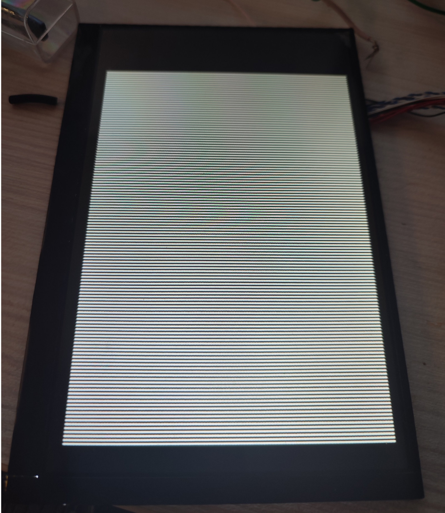
One interesting challenge: alternating single white/black pixel rows caused visible flickering on the composite output. The solution was to double each row (white-white-black-black pattern), which eliminated the flicker artifacts but halved the effective vertical resolution to 64 lines. This was an acceptable tradeoff for this application.
The PAL timing generator uses a state machine implementing:
- Broad sync sections
- Short sync sections
- Empty (blanking) lines
- Full data lines with pixel content
- Proper horizontal and vertical sync timing
Address calculation synchronizes memory access with the visible frame region: horizontal pixels span clock cycles 573-2971 per line, vertical lines 16-271 are visible, with 10 output pixels per source pixel horizontally and 4 source lines per destination line vertically.
Top-Level Module Architecture
The complete system consists of three main components:
- Decoder — captures GID signals, writes to SRAM port A
- SRAM — dual-port memory (8-bit write on port A, 1-bit read on port B)
- PAL — reads SRAM port B, generates composite video output
Debugging Challenges
The development process was far from smooth. I encountered numerous issues during simulation:
- Incorrect address mapping between the write port and read port
- Off-by-one errors in row calculations
- Timing misalignment between the decoder and PAL output modules
Extended modeling with iverilog proved invaluable for identifying and resolving these issues before deploying to actual hardware.
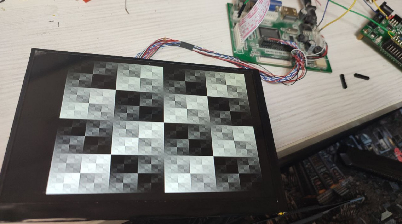
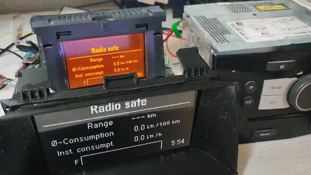
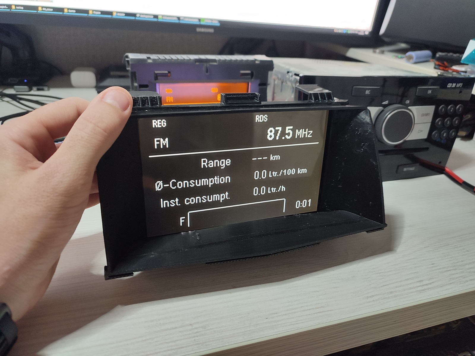
Results
The working system successfully:
- Decodes the GID display protocol in real-time
- Captures framebuffer data in FPGA SRAM
- Generates CVBS output compatible with aftermarket head units
- Preserves original GID functionality — the display continues to work normally in the vehicle

Conclusion
The project isn't perfectly optimized — it was built hastily over 3-4 evenings — but I'm very satisfied with the results and learned an immense amount in the process. The approach of intercepting display signals rather than decoding CAN bus messages proved to be an elegant solution that captures exactly what the driver sees on the original GID, regardless of what system is generating the content.
FAQ
What is this article about in one sentence?
This article explains the core idea in practical terms and focuses on what you can apply in real work.
Who is this article for?
It is written for engineers, technical leaders, and curious readers who want a clear, implementation-focused explanation.
What should I read next?
Use the related articles below to continue with closely connected topics and concrete examples.