Kilometer-Range Ethernet: Building a 10BASE-T1L Converter
A practical guide to building a 10BASE-T1L Ethernet media converter using the ADIN1100 transceiver, enabling 10 Mbps Ethernet over a single twisted pair at distances up to one kilometer.
Greetings, Habr!
So much has been said about the 10BASE-T1L standard, yet I haven't found a single practical implementation (I'm talking specifically about actual circuit design that you could use in your own device). And then, as if on cue, I needed to implement long-distance data transmission. DSL and RS-485 were considered as alternatives, of course, but since I needed to transmit audio, I decided to try 10BASE-T1L.
What Is 10BASE-T1L?
So, first things first: what exactly is 10BASE-T1L? It is an Ethernet physical layer standard (IEEE 802.3cg-2019) with a data rate of just 10 Mbps. But the link distance can reach one kilometer (according to some sources, up to two kilometers), and all of this over a single twisted pair of wires.
I found only two T1L transceiver chips: the DP83TD510ERHBR (from Texas Instruments) and the ADIN1100CCPZ (from Analog Devices). I chose the second option because I had previous experience with Analog Devices Ethernet PHYs and they performed well, plus they were available to order, which is very relevant these days.
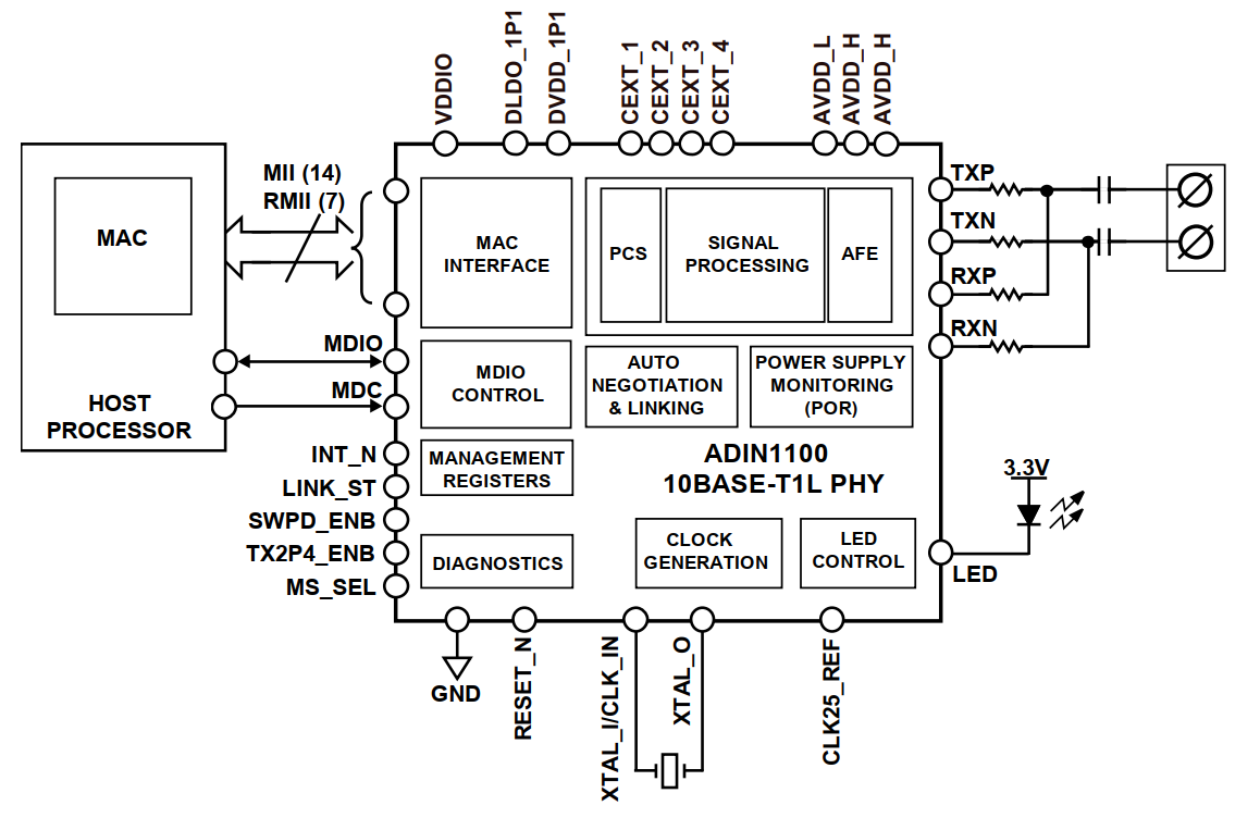
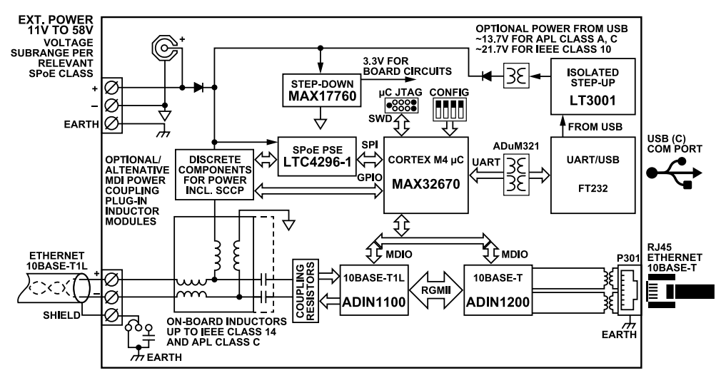
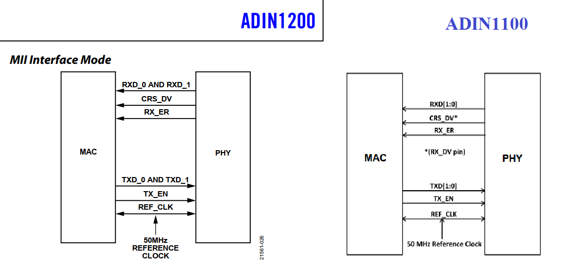
ADIN1100 Block Diagram
Looking at the block diagram (on the left), we can see that the chip needs a MAC-level MII/RMII interface from the host. Accordingly, in my design I can connect the chip directly to the processor/controller's RMII without any conversions. I'll go even further — you can make separate modules that, when installed, give you either 10BASE-T1L or standard 10/100/1000 Ethernet at the device output.
I managed to find a description of a kit called "DEMO-ADIN1100D2Z," which contained a block diagram. It shows that the evaluation board is built on two PHY chips connected via RGMII.
Design Approach
For testing and debugging the chip, it will be quite convenient to use double conversion: 10BASE-T <-> RMII <-> 10BASE-T1L (and back). This means you can develop a device as a standalone unit and try connections with different cables and between different devices. You can choose any second PHY, but the ADIN1100 + ADIN1200 pair costs about 1,000 rubles retail (at the moment), which is quite acceptable.
Since I don't need any software configuration of the chips, I can safely remove the microcontroller, USB/UART, and so on from this design. Power over Data Line (PoDL) isn't needed either, although the chip supports it.
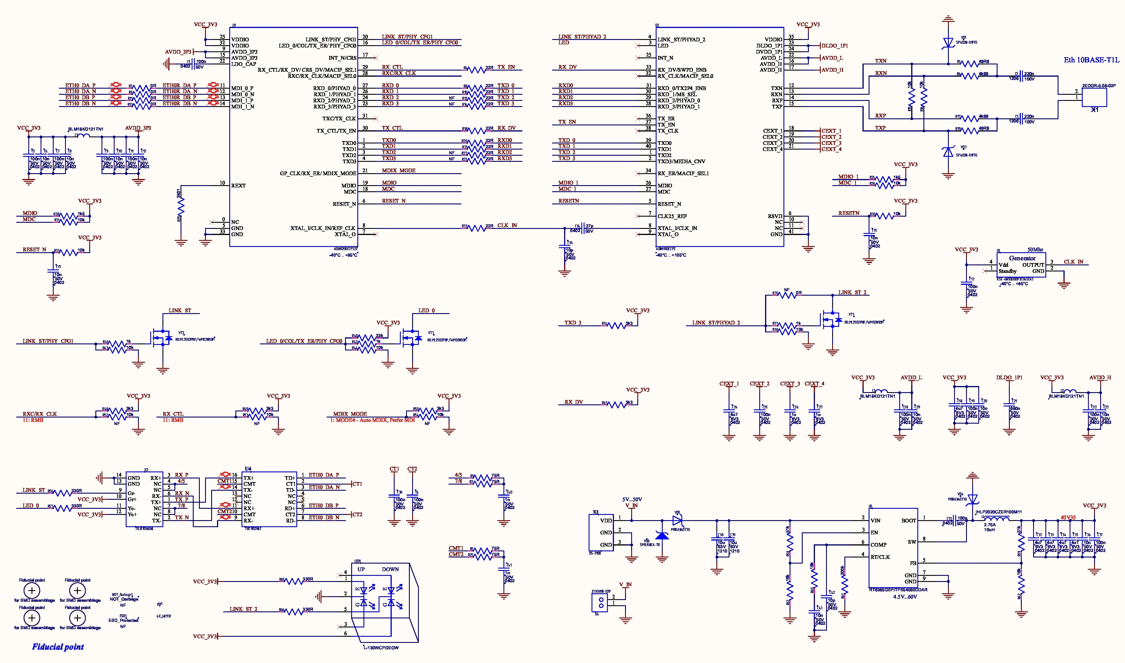
Both PHYs need just one external power supply of 3.3V. To get a wide input voltage range (up to 60V), I used a DC/DC converter TPS54560DDAR (from Texas Instruments), especially since a pin-to-pin analog has appeared — the RT6365GSP (from Richtek). This gives me just three ICs on the board.
Clocking the Chips
Looking at the datasheets for how to implement clocking for the chips — excellent. You can use a single 50 MHz oscillator.
Converter Schematic
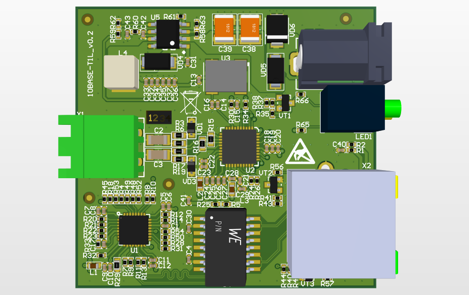
Below is the device schematic. The most observant readers may notice that the schematic differs somewhat from the board photo. I removed some configuration resistors (which definitely won't be needed going forward) and test points, since everything was debugged on the first board iteration.
Notably, the ADIN1100 is very sensitive to pull-up/pull-down resistors. I decided to optimize the schematic a bit with resistor values, but no luck. For example, a 1 kohm resistor won't work for the chip's reset signal, and 10 kohm resistors won't work for operating mode selection. I spent two days on this problem.
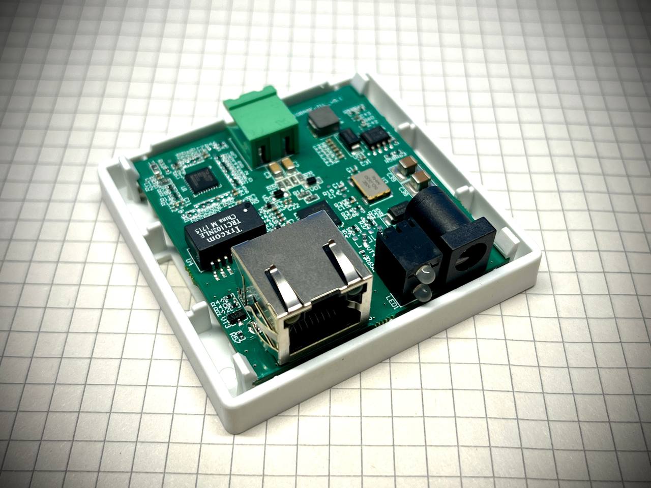
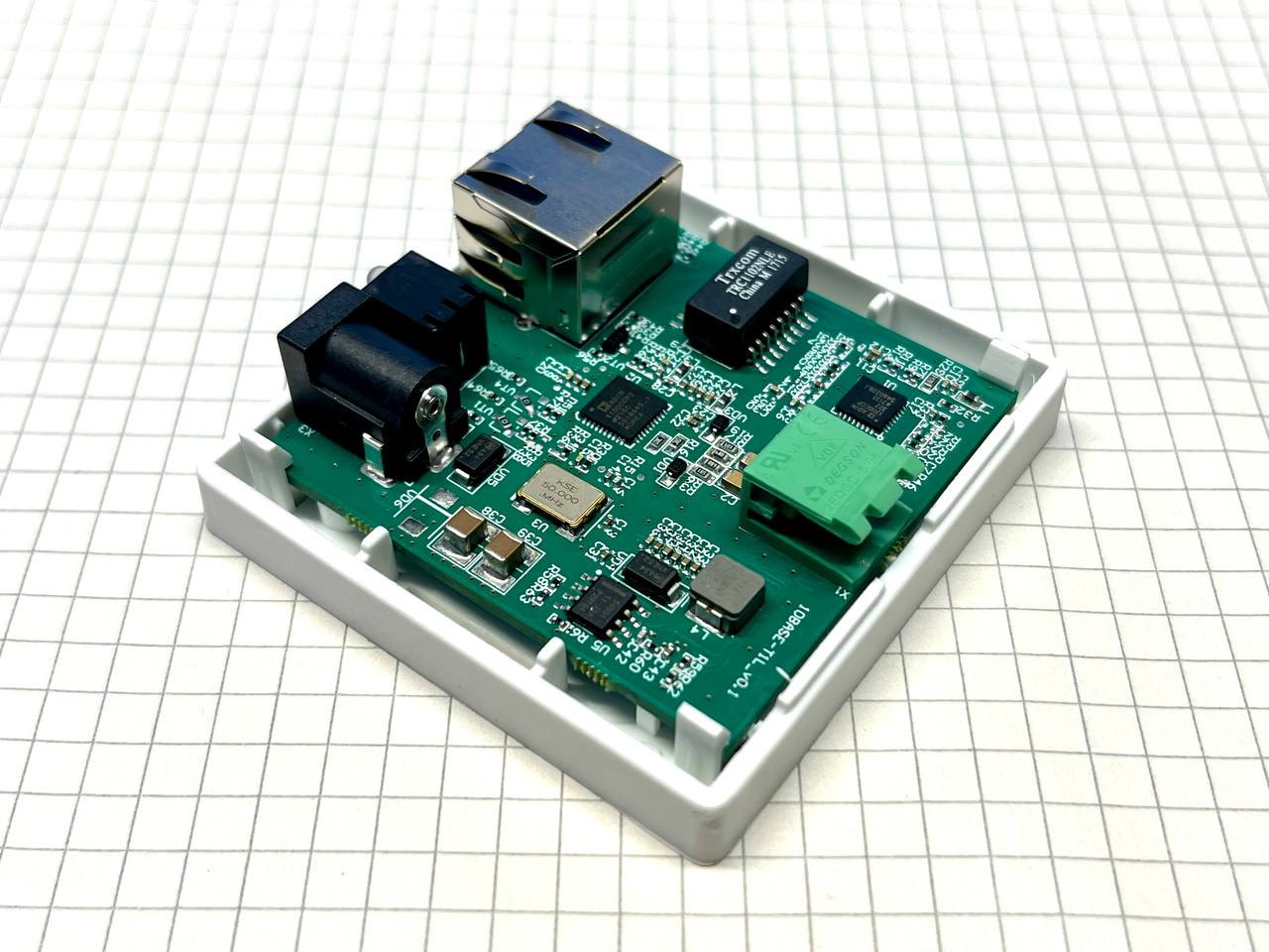
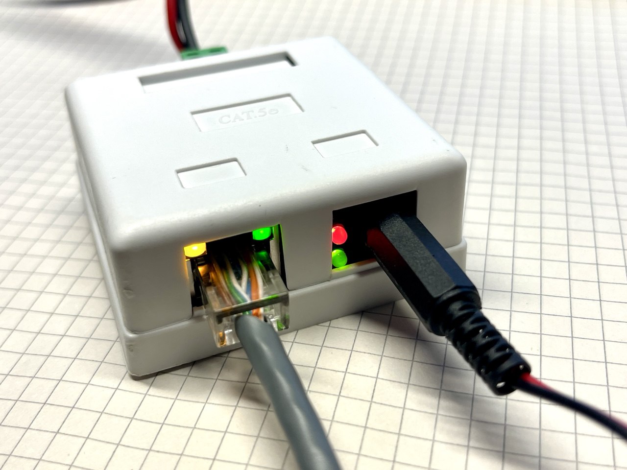
For testing convenience, and possibly for future use, I decided to lay out the board inside an Ethernet wall socket. I had a couple hundred sockets left over from a previous project.
Testing the Device
For testing, I used several spools of Cat.5e cable connected in series (one pair). The total length came out to 590 meters. Cable length from 56 meters to 590 meters had no effect on the connection speed. For receive/transmit, I got an average of 7-9 Mbps. I haven't figured out yet why it doesn't quite reach 10, although it does hit 12 at peak moments.
The first board iteration was done on four layers, but if you remove all unnecessary configuration, it's quite feasible to route on two layers. I've sketched out a new board (based on the schematic above), and it looks roughly like this. Single-sided mounting.
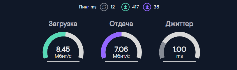
Surprisingly, with an internet speed of 20 Mbps, 8.5 Mbps on the PC feels quite normal for web browsing, but the goal is obviously not to extend the distance from the router to the computer.
I also decided to test with different cables. According to measurements, twisted pair performs better than regular wire, which makes sense.
The LEDs on the Ethernet connector show link and data status. Near the power connector, they show power presence and T1L link status respectively.
Conclusion
Summing up: it's entirely feasible to implement a long-range Ethernet line, even if at low speed. All you need is a pair of these converters and a long cable. I hope the device schematic will be useful to someone for their own projects.
Thank you for your attention, and good luck!