Inside Look: LCD and E-Ink Displays
A microscopic journey into the inner workings of LCD and E-Ink displays, examining their structure through optical and electron microscopy — from liquid crystals and color filters to e-ink microcapsules.
Foreword
Demain n'existe pas!
In the latest article from the "Inside Look" series, we discussed everyday things, but despite the abundance of material gathered in this direction over the past month, let's return to IT-related topics.
Specially for this occasion, LCD and E-Ink displays ended up on the dissection table — displays that had come to me in somewhat battered condition.
How Anton threw his phone against a wall, and the results of meticulous display teardowns — read on below.
Preface
Once upon a time there lived Anton Gorodetsky.
His wife left him, and he was deeply sad...
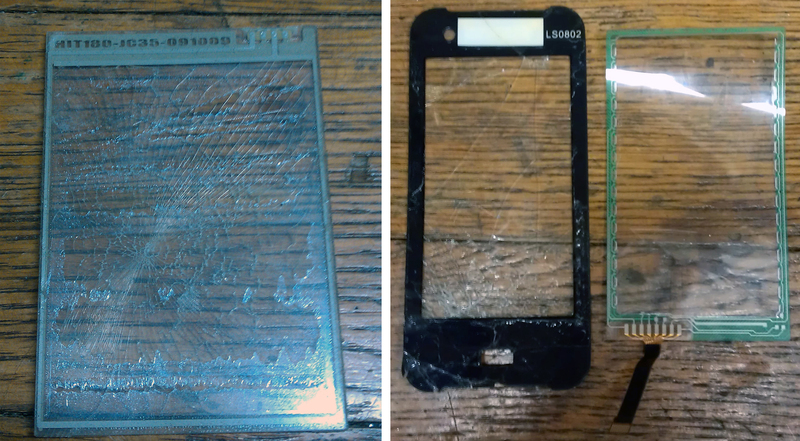
So begins the famous song by the band Umatturman. And so begins the story of display research. After the first publication on Habr, my friend — a graduate student at the Faculty of New Materials at Moscow State University — came to me and said: "I broke my mobile phone, would you like to cut it open?" I was surprised because this person always carried a cheap Chinese phone that I considered practically indestructible. Coming home one day, Anton habitually tossed his phone into the wardrobe but, apparently miscalculating, hit the display squarely on the shelf edge.
Realizing his laughable losses from the phone's demise and given his overall bad mood that day, he acted like a true gentleman, hurling the lifeless body of the phone against the concrete wall again and again. By the time the remains reached me, half the Chinese phone was simply missing, and the display was covered in a fine web of cracks.
I had to set it aside until better times (as I then assumed, until someone did the same thing with an iPhone or another touchscreen smartphone) and began working on HDDs and CDs, then light bulbs, flash drives, and so on.
Some time later, my neighbor brought me a cracked E-Ink display. His friend had broken the thin glass in a well-known e-reader (model number 601) during an airsoft game, apparently, and gave the reader away practically for free for repair and restoration.
Now this was more interesting — two technologies could be compared to each other, attempting to see RGB subpixels and microcapsules filled with charged particles. But I was hoping to get a smartphone with a capacitive sensor, to compare it with the resistive sensor of the Chinese phone.
And then Vasily (a scientific colleague from one of the faculty labs), having come to our Chemistry Department from Chernogolovka and seeing what I was actually doing with the electron microscope, said he was willing to sacrifice a phone from a well-known Korean manufacturer with a somewhat damaged display for disassembly and cutting, with the note "nothing is too much for the sake of science."
Despite all assurances that the sensor was capacitive, it turned out to be resistive — albeit of a more advanced design than the Chinese phone's touch panel. From this phone, an important part was extracted that awaits its turn for dissection — the photo/video camera matrix...
Theoretical Part
How Does an LCD Display Work?
We've all been using flat TVs, monitors, phones, and smartphones for so long that we've already forgotten that a good monitor once weighed 10-15 kilograms (we still have one such mastodon standing — and most importantly, it still works!).
All of this became possible thanks to century-old discoveries (liquid crystals were discovered in 1888) and technological development over the last 30-40 years (1968 — a device for displaying information using liquid crystals; 1970s — liquid crystals became widely available). Much about liquid crystals and LCD monitors can be found on Wikipedia.
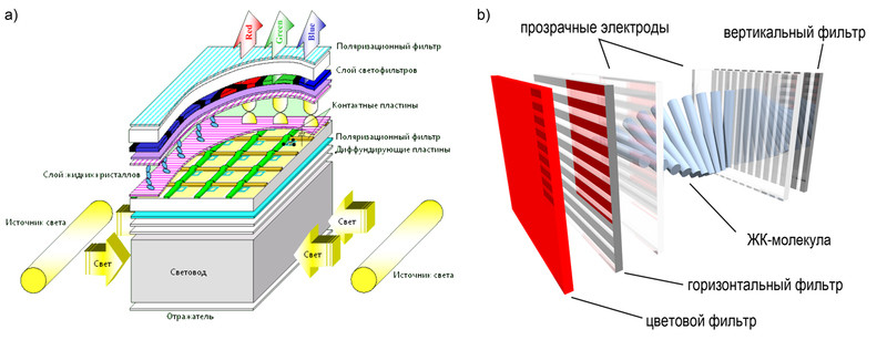
So, virtually any LCD monitor consists of the following main parts: an active matrix — a set of transistors that form the image; a liquid crystal layer with color filters that either pass light or don't; and a backlight system, which nowadays they're trying to fully convert to LEDs. Although my "aging" Asus G2S has a magnificent quality display backlit by fluorescent lamps.
How does all this work? Light from the source (LED or lamp) passes through a special transparent waveguide plate and is diffused so that the entire matrix has uniform brightness across its entire area. Then photons pass through a polarization filter that only allows waves with a specific polarization. After penetrating through a glass substrate where the active matrix of thin-film transistors is located, light reaches the liquid crystal molecule.
This molecule receives a "command" from the underlying transistor about what angle to rotate the light wave's polarization, so that after passing through another polarization filter, it sets the brightness of an individual subpixel. The color of each subpixel is determined by a layer of color filters (red, green, or blue). Mixing together, waves from three subpixels invisible to the human eye form an image pixel of the desired color and intensity.
This is demonstrated very clearly, in my opinion, in a video by Sharp.
In addition to the well-established LCD + TFT (thin-film transistors) technology, there is the actively promoted OLED + TFT technology, that is, AMOLED — active matrix OLED. The main difference is that the role of the polarizer, LC layer, and color filters is played by organic light-emitting diodes of three colors.
Essentially, these are molecules that can emit light when electric current flows through them, and depending on the amount of current, can change the intensity of their color — similar to how it works in regular LEDs. By removing the polarizers and LCs from the panel, we can potentially make it thinner and, most importantly, flexible!
What Types of Touch Panels Exist?
Since sensors are currently used mostly with LCD and OLED displays, I think it makes sense to talk about them right away.
A very detailed description of touchscreens or touch panels is given here, so I won't describe all types of touch panels — I'll focus only on the two main ones: resistive and capacitive.
Let's start with the resistive sensor. It consists of 4 main components: a glass panel (1) as the carrier for the entire sensor panel, two transparent polymer membranes with resistive coating (2, 4), a layer of micro-insulators (3) separating these membranes, and 4, 5, or 8 wires that are responsible for "reading" the touch.
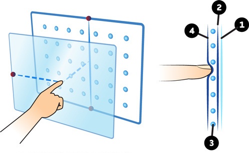
When we press such a sensor with a certain force, the membranes make contact, the electrical circuit closes as shown in the figure below, resistance is measured, which is then converted into coordinates:
It's all very simple.
It's important to remember two things: a) resistive sensors on many Chinese phones are not of high quality — this may be related to non-uniform spacing between membranes or poor-quality micro-insulators, meaning the phone's "brain" cannot adequately convert measured resistances into coordinates; b) such a sensor requires actual pressing — pushing one membrane down to the other.
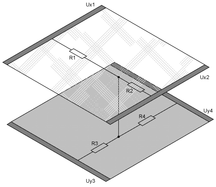
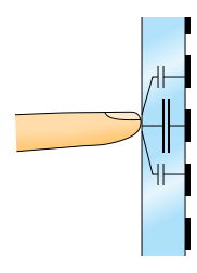
Capacitive sensors are somewhat different from resistive ones. It should be noted right away that we're talking only about projected capacitive sensors, which are now used in iPhones and other portable devices.
The operating principle of such a touchscreen is quite simple. A grid of electrodes is applied to the inner side of the screen, and the outer side is covered with, for example, ITO — a complex oxide of indium and tin. When we touch the glass, our finger forms a small capacitor with such an electrode, and the processing electronics measure the capacitance of this capacitor (applying a current pulse and measuring voltage).
Accordingly, a capacitive sensor only responds to firm contact with conductive objects — meaning touching such a screen with a nail will work intermittently, as will a hand soaked in acetone or dehydrated. Perhaps the main advantage of this touchscreen over a resistive one is the ability to make a fairly strong base — super-strong glass, like Gorilla Glass, for example.
How Does an E-Ink Display Work?
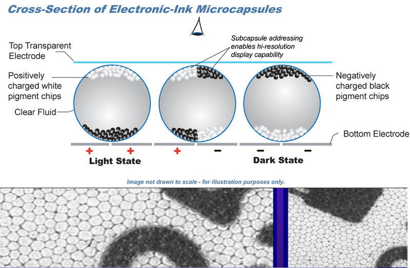
E-Ink is arguably much simpler in design compared to LCD. Again, we're dealing with an active matrix responsible for forming the image, but there are no liquid crystals or backlight lamps here whatsoever — instead, there are capsules with two types of particles: negatively charged black ones and positively charged white ones. The image is formed by applying a certain potential difference and redistributing particles within these micro-capsules, as clearly demonstrated in the figure below:
If that's not enough for someone, the working principle of electronic paper is demonstrated in this video.
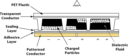
In addition to E-Ink technology, there is SiPix technology, which has only one type of particle, with the "fill" itself being black:
For those who seriously want to learn about "magnetic" electronic paper, please go here — there was once an excellent article in Perst.
Practical Part
Chinese Phone vs. Korean Smartphone (Resistive Sensor)
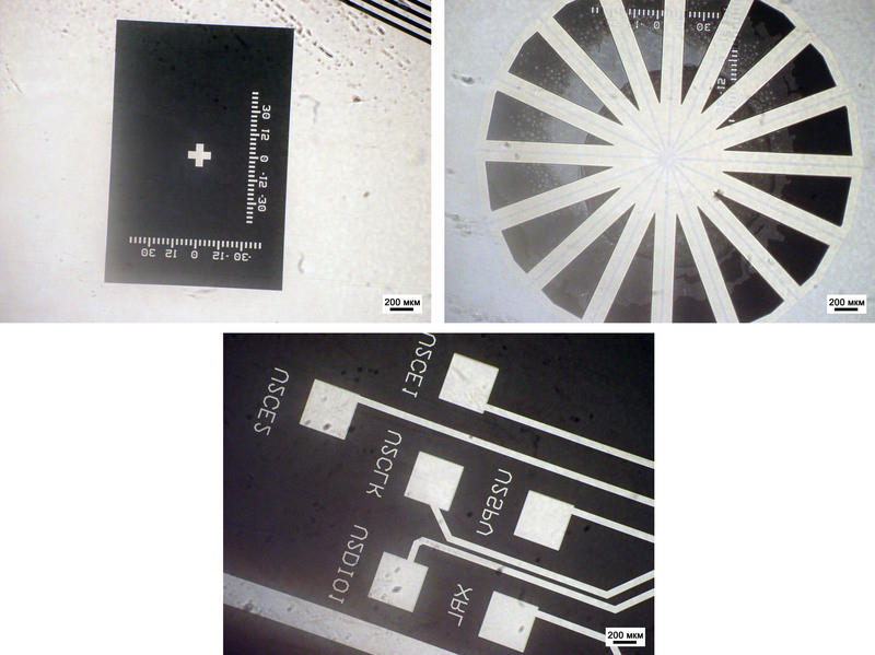
After "carefully" unscrewing what remained of the Chinese phone's board and display, I was greatly surprised to discover a mention of a well-known Korean manufacturer on the phone's motherboard:
I disassembled the screen carefully and gently — so that all polarizers remained intact. So I just had to play with them and with the working big brother of the specimen being prepared, and recall the optics lab practicum:
Note that the entire backlight relies on just four tiny LEDs (I think their total power is no more than 1 W).
Then I spent a long time looking for the sensor, sincerely believing it would be a fairly thick panel. It turned out to be completely the opposite. In both the Chinese and Korean phones, the sensor is several sheets of plastic that are very well and tightly glued to the outer panel glass:
The Chinese phone's resistive sensor is built on the "simpler is better" principle, unlike its more expensive South Korean counterpart. If I'm wrong, please correct me in the comments, but on the left in the picture is a typical 4-wire sensor, and on the right is an 8-wire sensor.
LCD Display of the Chinese Phone
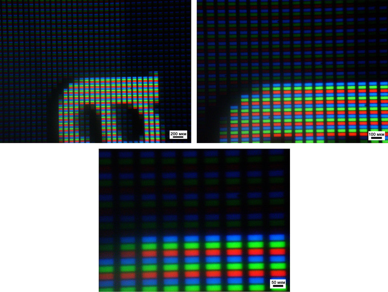
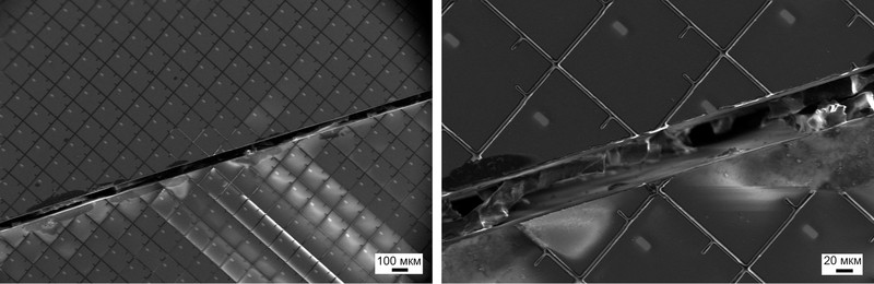
Since the Chinese phone's display was already broken and the Korean one was only slightly damaged, I'll use the first one to talk about LCD. But let's not break it completely just yet — let's look at it under an optical microscope:
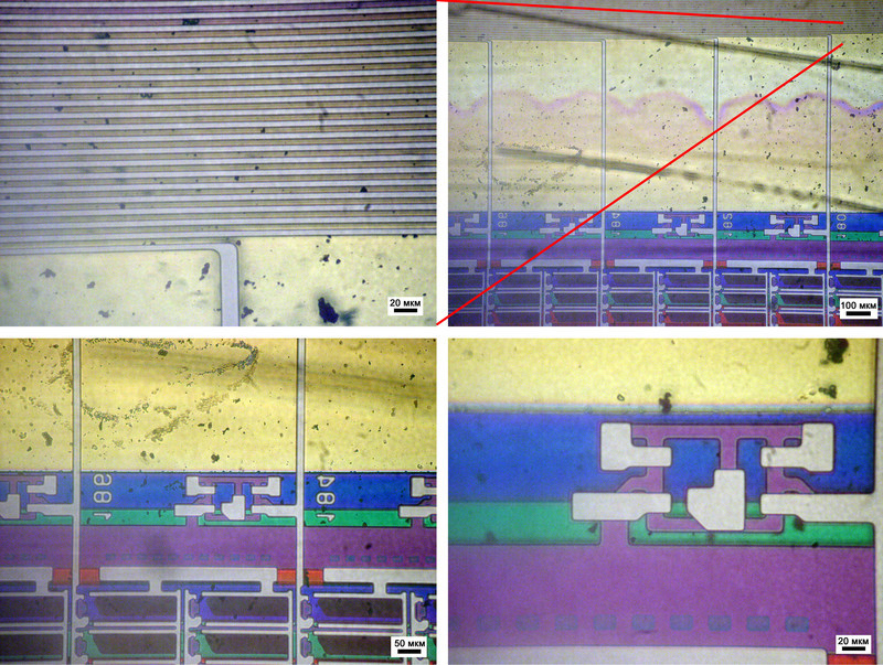
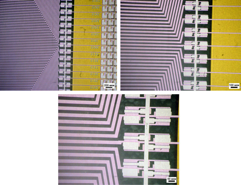
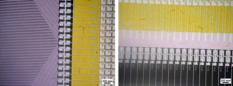
One wire powers two lines of pixels at once, and the isolation between them is achieved using a completely unusual "electrical bug" (bottom right photo). Behind this entire electrical circuit are color filter tracks painted in the corresponding colors: red (R), green (G), and blue (B).
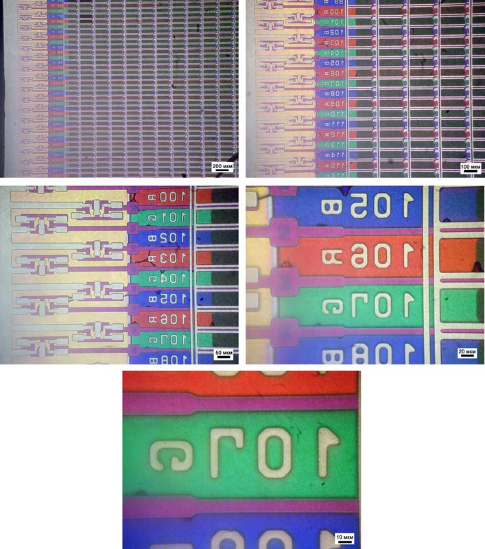
At the opposite end of the matrix from the ribbon cable attachment point, you can find a similar color breakdown, track numbers, and the same switches (if anyone could explain in the comments how this works, that would be great!):
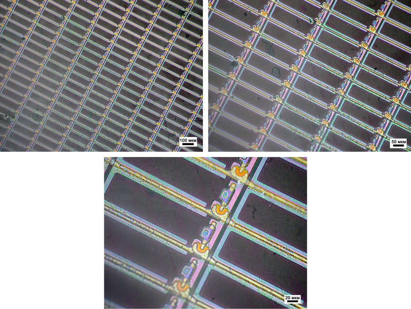
This is what a working LCD display looks like under a microscope in real life.
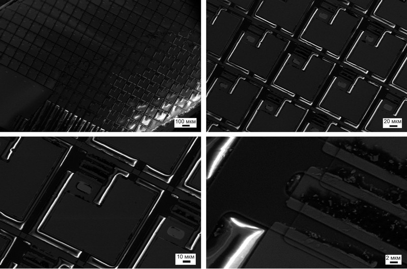
That's it — we won't see this beauty anymore. I literally crumbled it, and after struggling a bit, "split" one such crumb into two separate pieces of glass, which make up the main part of the display...
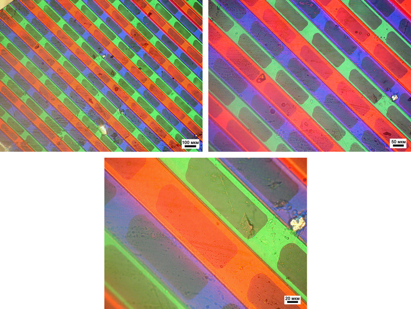
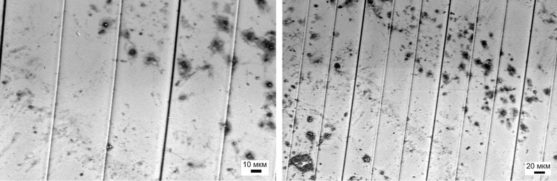
Now we can look at individual color filter tracks. I'll tell you about the dark "spots" on them a bit later:
And now a small methodological note regarding electron microscopy. The same colored stripes, but now under the electron microscope beam: the color has disappeared! As I mentioned earlier (for example, in the very first article), the electron beam is completely "color-blind" — it doesn't matter whether it interacts with colored material or not.
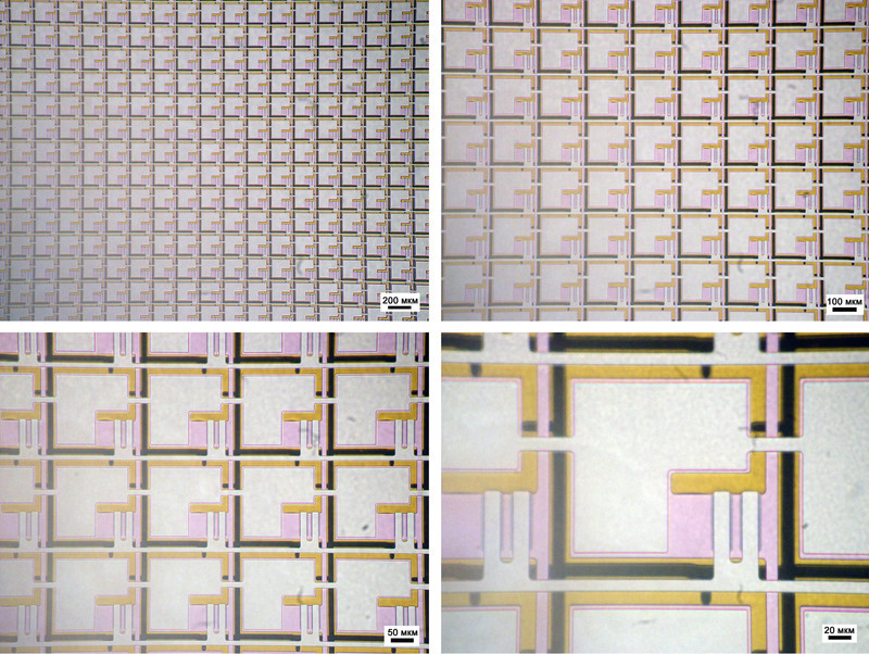
Let's also look at the reverse side. It houses the transistors:
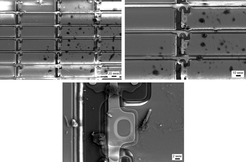
In the optical microscope this is slightly less visible, but SEM allows us to see the outline of each subpixel — this is quite important for the following conclusion.
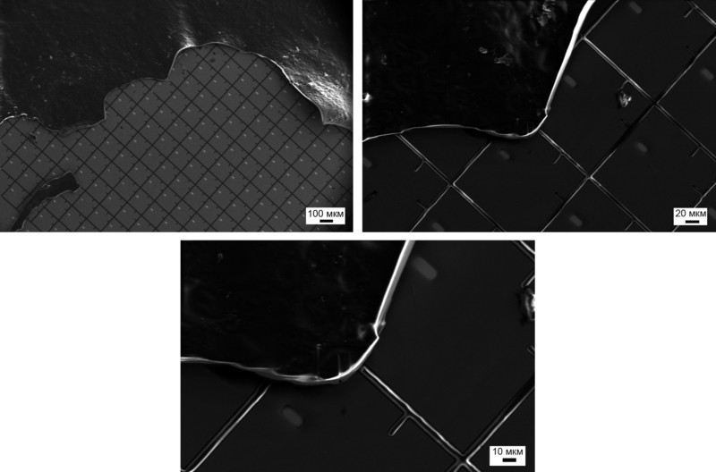
So, what are these strange dark areas?! I thought long and hard, racked my brain, read many sources (perhaps the most accessible was Wikipedia) and, by the way, that's why I delayed publishing the article on Thursday, February 23rd. And here is the conclusion I reached (I may be wrong — please correct me!).
In VA or MVA technology — one of the simplest, and I don't think the Chinese invented anything new here: each subpixel must be black. That is, light doesn't pass through it (here's an example of a working and non-working display). Considering that in the "normal" state (without external influence), the liquid crystal is disoriented and doesn't provide the "needed" polarization, it's logical to assume that each individual subpixel has its own LC film.
Thus, the entire panel is assembled from individual micro-LCD displays. The observation about each subpixel having its own outline fits organically here. For me, this was a kind of unexpected discovery made right during article preparation!
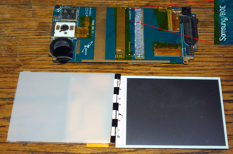
I felt sorry for breaking the Korean phone's display — after all, I need something to show children and visitors who come to our faculty for tours. I don't think we could have seen anything else interesting.
Next, just for fun, here's an example of pixel "organization" from two leading communicator manufacturers: HTC and Apple. An iPhone 3 was donated for a painless operation by one kind person, and the HTC Desire HD is actually mine:
A small note about the HTC display: I wasn't specifically looking, but could this stripe in the middle of the top two microphotographs be part of that very capacitive sensor?!
If memory serves me right, HTC has a superLCD display, while iPhone 3 has a regular LCD. The so-called Retina Display — an LCD where both contacts for switching the liquid crystal lie in the same plane (In-Plane Switching — IPS) — is installed in iPhone 4.
I hope that soon an article comparing different display technologies will be published with 3DNews support. For now, I just want to note the fact that the HTC display is truly unusual: the contacts to individual subpixels are routed in a non-standard way — from the top somehow, unlike iPhone 3.
And lastly in this section, I'll add that the dimensions of one subpixel for the Chinese phone are 50 by 200 micrometers, for HTC — 25 by 100 micrometers, and for iPhone — 15-20 by 70 micrometers.
E-Ink from a Well-Known Ukrainian Manufacturer
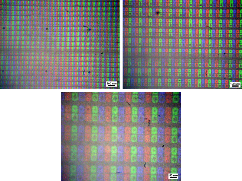
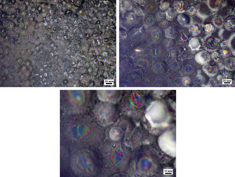
Let's start, perhaps, with the basics — "pixels," or more precisely cells, which are responsible for forming the image:
The size of such a cell is about 125 micrometers. Since we're looking at the matrix through the glass on which it's applied, please note the yellow layer in the "background" — that's a gold coating, which we'll need to remove later.
Next, the power supply contacts. This photo particularly impressed me:
Among other things, many interesting items were found on the glass substrate. For example, positioning marks and contacts that are apparently intended for testing the display during manufacturing:
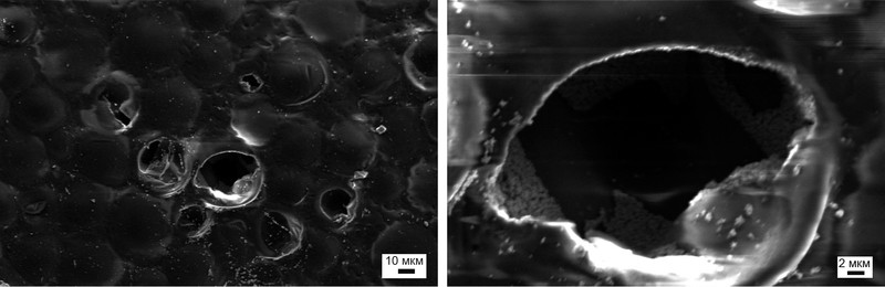
Of course, this doesn't happen often and is usually an accident, but displays sometimes break. For example, this barely visible crack thinner than a human hair can permanently deprive you of the joy of reading your favorite book about foggy Albion in the stuffy Moscow metro:
By the way, here it is — the gold I mentioned — a smooth pad "underneath" the cell for quality contact with the ink (more about that below). We remove the gold mechanically and here's the result:
Hidden under the thin gold film are the control components of the active matrix, if we can call it that.
But the most interesting part, of course, is the "ink" itself:
Of course, it's hard to find even one destroyed microcapsule to look inside and see the "white" and "black" pigment particles.
Or maybe there IS something inside?!
The size of individual spheres — essentially an analog of a subpixel in E-Ink — can be as small as 20-30 micrometers, which is significantly smaller than the geometric dimensions of subpixels in LCD displays. Given that such a capsule can work at half its size, the image on good, high-quality E-Ink displays turns out to be much more pleasant than on LCD.
Conclusion
At the end of my narrative, I would like to thank those who helped me writing this article: Anton (the broken Chinese phone is his handiwork), Alexey (the damaged E-Ink, rescued in time from the clutches of the repair service), Vasily (for the Korean phone, whose camera will be the hero of one of the next publications), Masha (who wasn't afraid to give me her iPhone), and Katerina (for living up to her surname).
P.S. In the end, I managed to grab a small piece of the reader and study the flexible electronics technology.