End of the Silicon Era? China Launches Production of Molybdenum Disulfide Chips
China has launched an engineering demonstration line in Shanghai for processors based on molybdenum disulfide, a two-dimensional material just three atoms thick that could overcome silicon's fundamental scaling limits.
Changes are brewing in the semiconductor industry. Humanity is approaching the limits of silicon. This material has been the foundation of technological progress for decades, but further transistor shrinkage is increasingly accompanied by current leakage, rising heat dissipation, and manufacturing complexity. China is betting on ultra-thin two-dimensional materials as a possible basis for the next stage of miniaturization and energy efficiency.
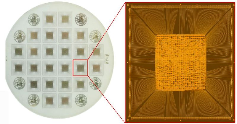
In early 2026, an engineering demonstration line for producing processors based on molybdenum disulfide was launched in Shanghai. The project is being developed by Shanghai Atomic Technology, a company founded in February 2025 by Professor Bao Wenzhong from Fudan University. The transition to full-scale production is planned to begin in June 2026.
The WUJI Processor: From Prototype to Production
Development began in the laboratories of Fudan University several years ago. A team led by Professors Peng Zhou and Bao Wenzhong worked on integrating two-dimensional semiconductors into full-fledged circuits. In spring 2025, they presented a 32-bit processor on the RISC-V architecture, named RV32-WUJI.
Chip Specifications
- Transistor channels made from molybdenum disulfide
- Material grown in monomolecular layers on a sapphire substrate
- A single chip contains 5,931 transistors (a world record)
- Chip size: 6 x 6 mm
- Operating frequencies: kilohertz range
- Power consumption: approximately 0.43 milliwatts
WUJI Functionality
- Fully executes 32-bit RISC-V instructions
- Correctly performs arithmetic operations with numbers up to 4.2 billion
- Supports gigabyte-scale data addressing
- Contains a complete set of basic blocks: arithmetic logic unit, registers, instruction decoder, and control logic
Technological Solutions
- All transistors are n-type
- Threshold voltage is tuned using different gate metals (aluminum and gold)
- Optimized dielectric layer
- Approximately 70% of technological steps are compatible with silicon production lines
- Key processes are protected by more than 20 patents
Standard Cell Library
The team created a library of 25 standard logic cells, enabling the design of more complex digital blocks and architectural scaling.
Testing
In tests, the processor performed symbolic operations:
- 1946 + 25 = 1971 (a reference to ENIAC)
- 1971 + 53 = 2025 (the year the Intel 4004 appeared... plus the current year)
Developments in 2025
- Integration of 2D memory with a silicon circuit using the ATOM2CHIP method
- An FPGA based on molybdenum disulfide with radiation resistance up to 10 megarads (for space and defense applications)

Properties of Molybdenum Disulfide and Why It Is Promising

Material Structure
- An atomic layer of molybdenum is sandwiched between two layers of sulfur
- Total thickness: just three atoms
- The material surface has no dangling bonds
Electrical Properties
- Ultra-thin transistor channel
- Dramatically improved electrostatic control
- Suppresses short-channel effects
- Low levels of defects and parasitic leakage
- Channel length and contacts below 35 nm achieved by late 2025
Advantages
- Transistors retain semiconductor properties at atomic channel thickness
- Lower energy losses and heat dissipation compared to scaled silicon
- High radiation resistance
- Mechanical flexibility
Applications
- Energy-efficient electronics
- Sensors and autonomous devices
- Specialized computing blocks
- Environments critical for power consumption and thermal management
Manufacturing Compatibility
The material can already be grown on industrial-format wafers. Many stages of the technology are compatible with CMOS processes.
Roadmap (According to Bao Wenzhong)
- 2026: Equivalent to 90-nanometer silicon process
- Next: Equivalent to 28 nm
- Prospect: Approaching 5-3 nm
Current Research
- Transistors without traditional dielectrics
- Improved doping methods to enhance carrier mobility
What Is Happening with Silicon Alternatives Worldwide
USA and Europe
- Active research on molybdenum disulfide transistors and other two-dimensional materials
- In summer 2025, Penn State University presented a fully non-silicon 2D computer based on molybdenum disulfide and tungsten diselenide (thousands of transistors of each type)
- American-Indian groups demonstrated highly efficient prototypes (at low operating frequencies)
Major Companies
- Samsung: Plans to transition to glass substrates in chip packaging by 2028
- USA and Europe: Experiments with graphene for interconnects and photonic computing circuits
- Russia: Primary focus on silicon carbide for power electronics
- India: Considering two-dimensional materials as an opportunity to close the technological gap
- Global trend: Growing interest in gallium nitride and other wide-bandgap semiconductors for high-power and high-voltage devices
The Role of Silicon
Silicon will not disappear in the coming years — its ecosystem is well-developed and its production scale is enormous.
Key Takeaway
The Shanghai project demonstrates that alternatives are beginning to move beyond laboratory experiments. If the announced roadmap is even partially realized, the first commercial devices based on two-dimensional materials could appear significantly earlier than expected.